Capacitative element, integrated circuit and electronic device

a technology of capacitors and components, applied in the field of capacitors, can solve the problem of not providing a highly reliable capacitor, and achieve the effect of large recording density

Inactive Publication Date: 2007-03-01
FUJITSU LTD
View PDF18 Cites 10 Cited by
  • Summary
  • Abstract
  • Description
  • Claims
  • Application Information

AI Technical Summary

Benefits of technology

[0006] However, BiFeO3 has a large leakage current for a ferroelectric material, and by itself cannot provide a highly reliable capacitor. It is an object of the present invention to reduce the leakage current of BiFeO3 while maintaining a Curie temperature higher than that of PZT, thereby providing a high-performance, high-capacity capacitive element containing no lead, along with an integrated circuit, semiconductor device and other electronic devices having this element.
[0010] With the present invention it is possible to achieve a high-performance semiconductor device or other electronic device with a large recording density which is environmentally friendly because it contains no lead.

Problems solved by technology

However, BiFeO3 has a large leakage current for a ferroelectric material, and by itself cannot provide a highly reliable capacitor.

Method used


Image

  • Capacitative element, integrated circuit and electronic device
  • Capacitative element, integrated circuit and electronic device
  • Capacitative element, integrated circuit and electronic device

Examples


example 1

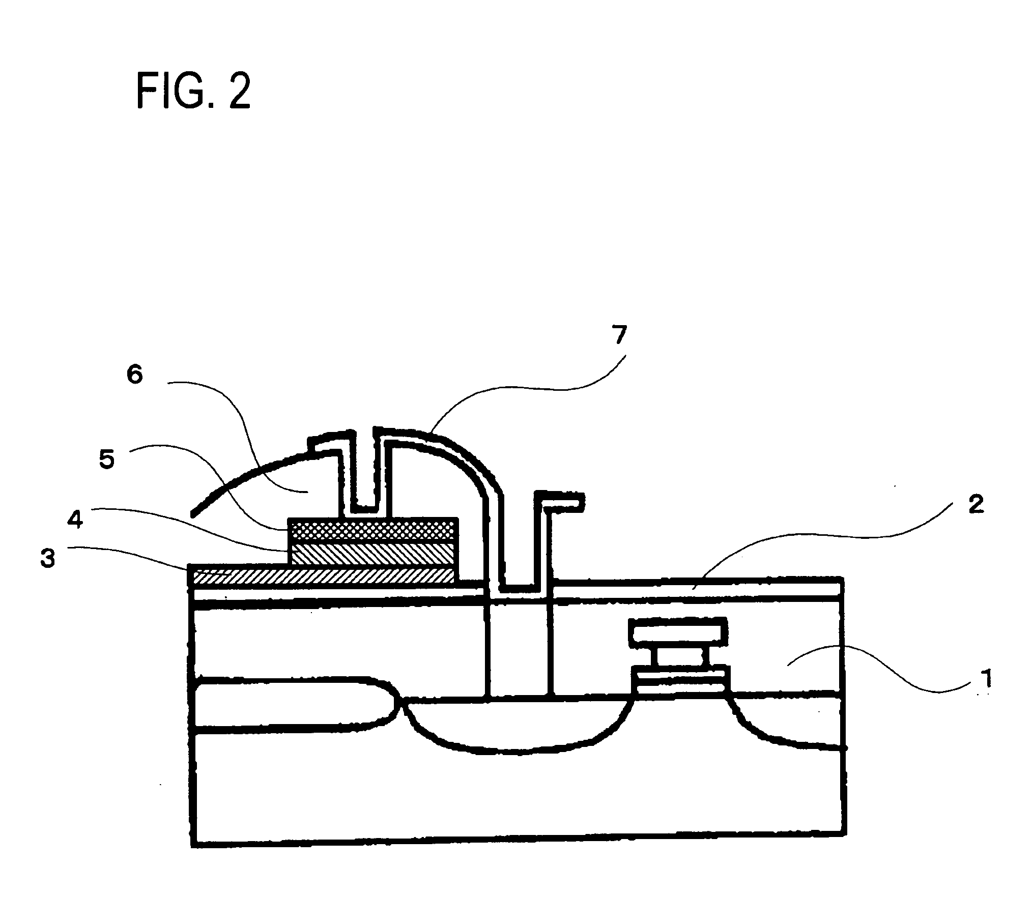
[0036] An electronic device (ferroelectric memory) having the structure of FIG. 2 can be manufactured by the following process. FIG. 2 is a model cross-section showing a 1C1T ferroelectric memory part.

[0037] (1) Silicon oxide film 2 is formed atop wafer 1 having a transistor formed thereon.

[0038] (2) A titanium oxide layer (not shown) as an adhesion layer and then a platinum layer as an underlayer electrode 3 are formed by sputtering.

[0039] (3) (Bi0.9, Ce0.1)FeO3 layer 4 is formed by MOCVD.

[0040] (4) A platinum layer is formed by vacuum deposition as an upper electrode 5.

[0041] (5) Patterning is then performed by photolithography.

[0042] (6) The whole is covered with silicon oxide film 6, and the upper electrode is taken to the surface to form a wiring layer 7.

example 2

[0043] An electronic device (ferroelectric memory) having the structure of FIG. 3 can be manufactured by the following process. FIG. 3 is a model cross-section showing an FET ferroelectric memory part.

[0044] (1) Two inch silicon monocrystalline substrate 11 having (001) orientation is washed and soaked in 9% weight dilute hydrofluoric acid to remove the SiOx layer from the substrate surface.

[0045] (2) The silicon monocrystalline substrate is set in a film-forming chamber and maintained at an actual substrate temperature of 550° C., and a YSZ (yttrium stabilized zirconia) target is irradiated with a KrF excimer laser at a pressure of 7×10⁻² Pa in a 12 sccm flow of oxygen (gas flow per minute (mL / minute) at 20° C., 1 atmosphere) to epitaxially grow YSZ film 12 to 5 nm by pulse laser deposition.

[0046] (3) The crystal structure of the ferroelectric layer of the present invention can be directly formed on a YSZ film, but in that case the orientation will be (101) and the polarization ...

example 3

[0053] A 1T1C ferroelectric memory can be obtained as in Example 1 by forming a (Bi0.8, Nd0.2)FeO3 layer or a Bi (Fe0.9Sc0.1)O3 layer in place of the (Bi0.9, Ce0.1)FeO3 layer.


PUM

PropertyMeasurementUnit
Curie temperatureaaaaaaaaaa
melting pointaaaaaaaaaa

Abstract

The present invention provides a capacitive element comprising BiFeO3 having particular cations other than Bi ions or Fe ions at the Bi ion sites or Fe ion sites of a crystal lattice, along with an electronic device and the like using that capacitive element. According to the present invention, it is possible to achieve a high-performance electronic device which has a large recording density and which is environmentally friendly because it contains no lead.

Description

CROSS REFERENCE TO RELATED APPLICATIONS [0001] This application is a continuation of International Application No. PCT / JP2004 / 008561, filed on Jun. 11, 2004, now pending, herein incorporated by reference.TECHNICAL FIELD [0002] The present invention relates to a capacitive element for use in non-volatile semiconductor memories and the like. BACKGROUND ART [0003] It is expected that non-volatile memories (FeRAM) using ferroelectrics with spontaneous polarization for the capacitor part will be applied as next-generation memories to non-contact IC cards and the like. This kind of capacitor is desirable from a practical standpoint because it allows for a wider operating margin, the greater the amount of polarization is. [0004] At present, PZT (lead zirconate titanate: PbZr1-xTixO3) materials are used as ferroelectric capacitor materials for obtaining large polarization. PZT is an oxide containing lead, and since lead is a toxin that accumulates in the human body it is desirable that its ...

Claims


Application Information

Patent Timeline
Patent Type & Authority Applications(United States)
IPC IPC(8): H01B1/12C04B35/26C04B35/453H01L27/105H01L27/115
CPCH01L27/11502C04B35/26H10B53/00
Inventor KONDO, MASAO
Owner FUJITSU LTD
Why Eureka
Try Eureka