Ultra-thin body vertical tunneling transistor

a transistor and ultra-thin body technology, applied in the field of transistors, can solve the problems of affecting performance, draining batteries, and so small transistor lengths

Active Publication Date: 2007-03-01
MICRON TECH INC
View PDF32 Cites 21 Cited by
  • Summary
  • Abstract
  • Description
  • Claims
  • Application Information

AI Technical Summary

Problems solved by technology

Transistor lengths have become so small that current continues to flow when they are turned off, draining batteries and affecting performance.
Sub-threshold leakage currents are difficult to control and reduce in conventional nano-scale planar complementary metal oxide semiconductor (CMOS) transistor technology.
As technology scales, sub-threshold leakage currents can grow exponentially and become an increasingly large component of total power dissipation.
At such power levels, there will not be enough voltage range to turn on a transistor.
With a 1.2 V voltage range, there will not be enough voltage swing to allow both objectives: high on current and low sub-threshold leakage to be accomplished with conventional planar devices.
This allows best control over the transistor channel but the structure has been difficult to realize in practice.
None of these techniques, however, can have a sub-threshold slope less than the ideal characteristic of 60 mV / decade for a convention MOSFET.

Method used


Image

  • Ultra-thin body vertical tunneling transistor
  • Ultra-thin body vertical tunneling transistor
  • Ultra-thin body vertical tunneling transistor

Examples


Embodiment Construction

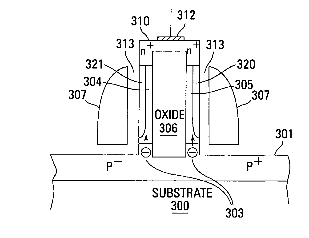
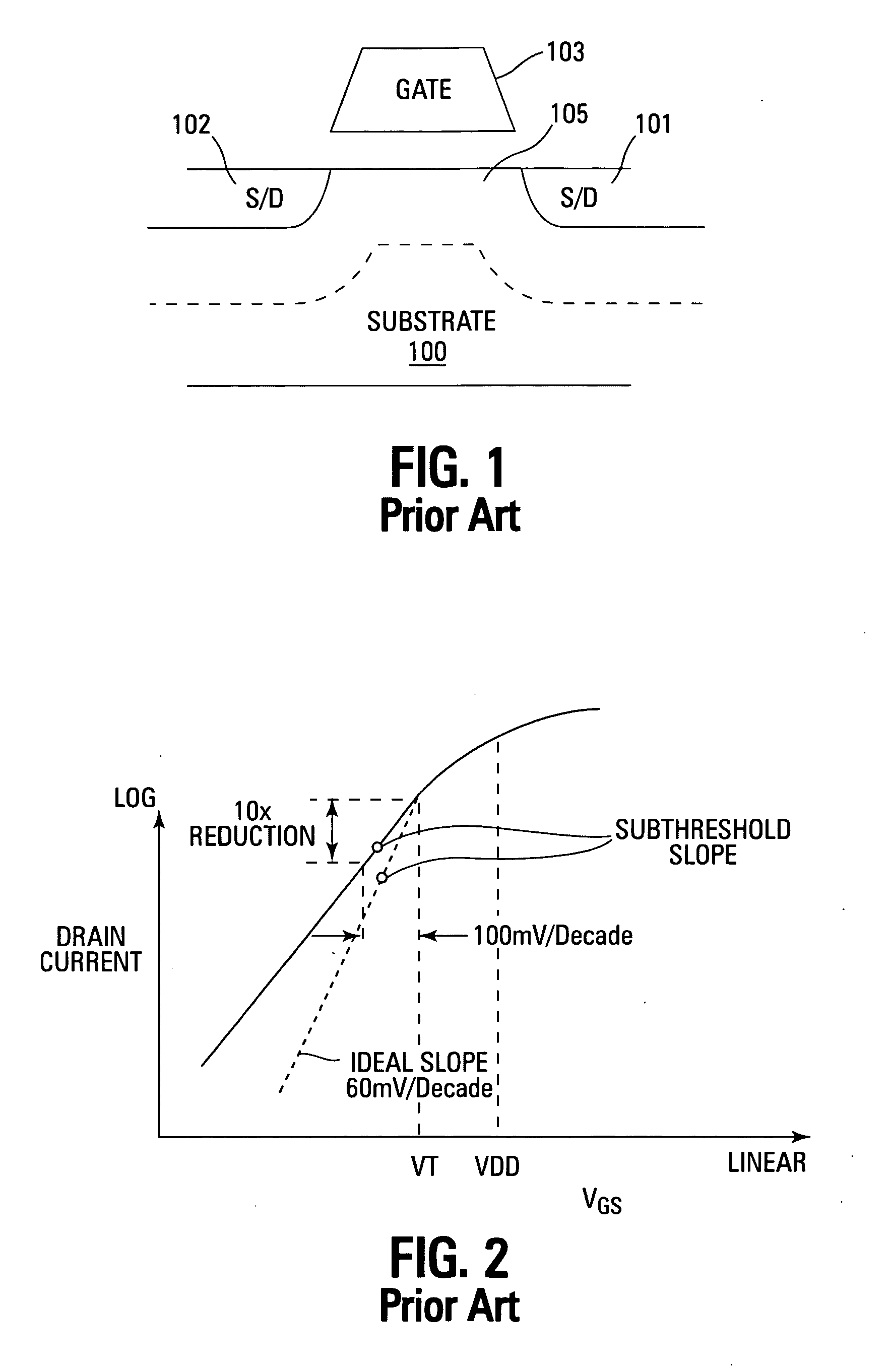
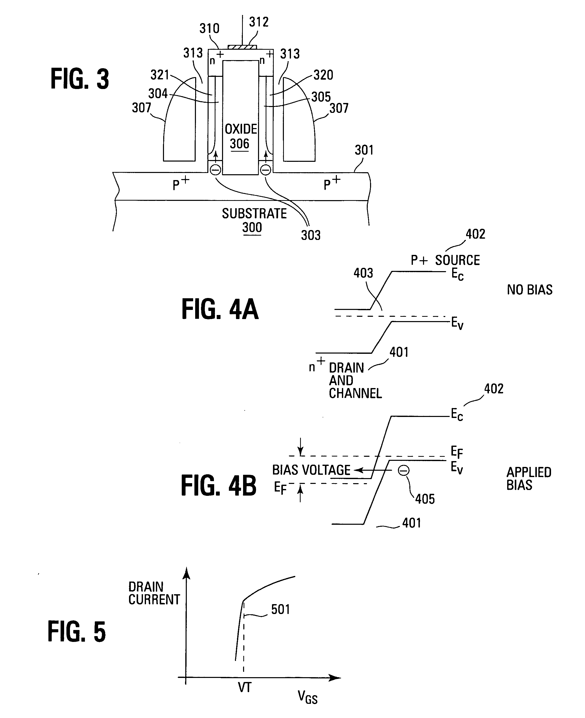
[0026] In the following detailed description of the invention, reference is made to the accompanying drawings that form a part hereof and in which is shown, by way of illustration, specific embodiments in which the invention may be practiced. In the drawings, like numerals describe substantially similar components throughout the several views. These embodiments are described in sufficient detail to enable those skilled in the art to practice the invention. Other embodiments may be utilized and structural, logical, and electrical changes may be made without departing from the scope of the present invention. The following detailed description is, therefore, not to be taken in a limiting sense, and the scope of the present invention is defined only by the appended claims and equivalents thereof. The terms wafer or substrate used in the following description include any base semiconductor structure. Both are to be understood as including silicon-on-sapphire (SOS) technology, silicon-on-...


PUM


Abstract

A vertical tunneling, ultra-thin body transistor is formed on a substrate out of a vertical oxide pillar having active regions of opposing conductivity on opposite ends of the pillar. In one embodiment, the source region is a p+ region in the substrate under the pillar and the drain region is an n+ region at the top of the pillar. A gate structure is formed along the pillar sidewalls and over the body layers. The transistor operates by electron tunneling from the source valence band to the gate bias-induced n-type channels, along the ultra-thin silicon bodies, thus resulting in a drain current.

Description

TECHNICAL FIELD OF THE INVENTION [0001] The present invention relates generally to electronic components and in particular the present invention relates to transistors. BACKGROUND OF THE INVENTION [0002] Transistor lengths have become so small that current continues to flow when they are turned off, draining batteries and affecting performance. When the gate-source voltage, Vgs, of a metal oxide semiconductor (MOS) transistor is less than its voltage threshold, Vt, it is in the sub-threshold region. This is characterized by a exponential change in drain current with Vgs. Sub-threshold leakage currents are difficult to control and reduce in conventional nano-scale planar complementary metal oxide semiconductor (CMOS) transistor technology. As technology scales, sub-threshold leakage currents can grow exponentially and become an increasingly large component of total power dissipation. This is of great concern to designers of handheld or portable devices where battery life is important...

Claims


Application Information

Patent Timeline
Patent Type & Authority Applications(United States)
IPC IPC(8): H01L29/76H01L29/94H01L31/00
CPCH01L29/88H01L29/7391
Inventor FORBES, LEONARD
Owner MICRON TECH INC
Why Eureka
Try Eureka