Signal adder circuit capable of removing effects due to phase error or amplitude error of I and Q signals

a technology of adder circuit and adder circuit, which is applied in the direction of pulse technique, reradiation, instruments, etc., can solve the problems of adverse effect on subsequent signal processing

Inactive Publication Date: 2007-03-01
ALPS ALPINE CO LTD
View PDF2 Cites 3 Cited by
  • Summary
  • Abstract
  • Description
  • Claims
  • Application Information

AI Technical Summary

Benefits of technology

[0011] The present invention has been finalized in view of the drawbacks inherent in the conventional signal adder circuit and it is an object of the present invention to provide a signal adder circuit

Problems solved by technology

When the I and Q signals including the phase error or the amplitude error are added by the adder 10, a baseband signal

Method used


Image

  • Signal adder circuit capable of removing effects due to phase error or amplitude error of I and Q signals
  • Signal adder circuit capable of removing effects due to phase error or amplitude error of I and Q signals
  • Signal adder circuit capable of removing effects due to phase error or amplitude error of I and Q signals

Examples


Embodiment Construction

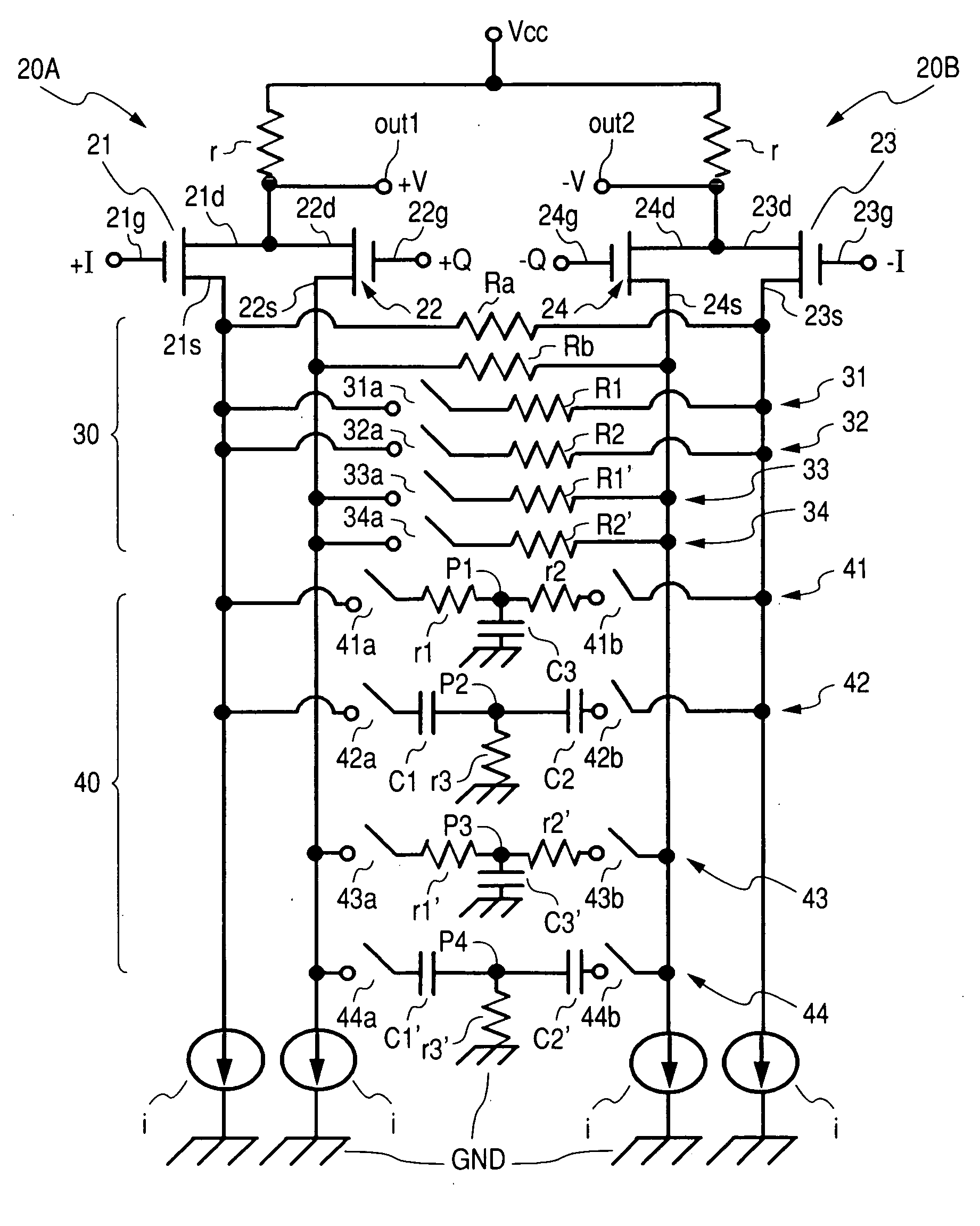
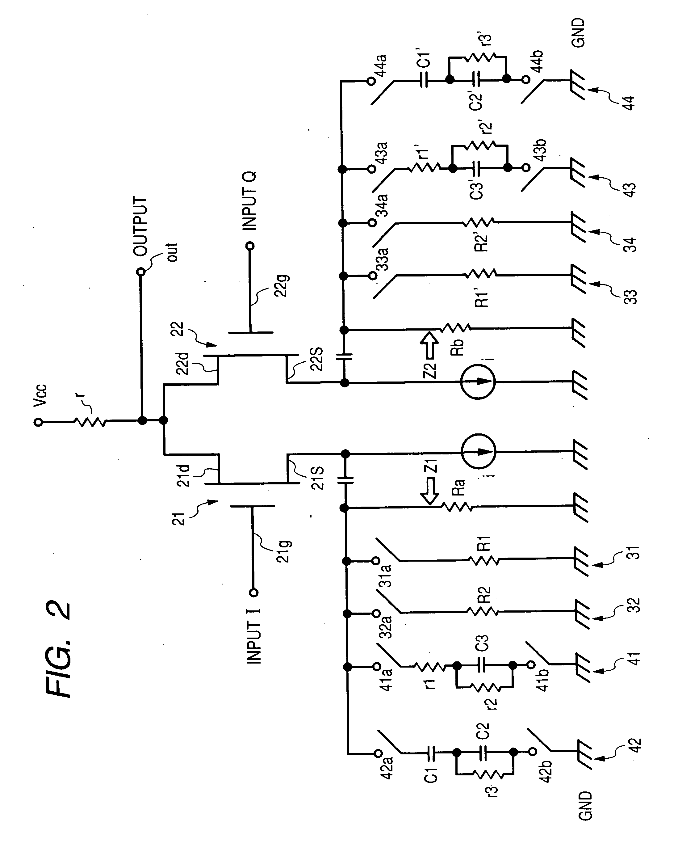
[0028]FIG. 1 is a circuit diagram showing a signal adder circuit according to an embodiment of the present invention and FIG. 2 is a circuit diagram showing an equivalent circuit of the signal adder circuit of FIG. 1. FIG. 2 shows one of two adders.

[0029] As shown in FIG. 1, a signal adder circuit 20 mainly includes an adder, a gain control unit, and a phase control unit.

[0030] The adder is formed by a semiconductor device such as an MOSFET and includes a first amplification element 21, a second amplification element 22, a third amplification element 23, and a fourth amplification element 24.

[0031] A first adder 20A is formed by a pair of the first amplification element 21 and the second amplification element 22 shown in a left upper side of FIG. 1. A second adder 20B is formed by a pair of the third amplification element 23 and the fourth amplification element 24 shown in right upper side of FIG. 1.

[0032] The first amplification element 21 is provided for the +I signal, the sec...


PUM


Abstract

A signal adder circuit includes: an adding unit that includes at least a pair of amplification elements in which a constant current flows between ground terminals and a ground, input signals having different phases are input to input terminals, and output terminals to which a power supply voltage is applied are connected to each other; a gain control unit that is provided between the ground and each of the ground terminals of the amplification elements so as to adjust the amplitudes of the input signals having different phases; and a phase control unit that is provided between the ground and each of the ground terminals of the amplification elements so as to adjust the phases of the input signals having different phases.

Description

BACKGROUND OF THE INVENTION [0001] 1. Field of the Invention [0002] The present invention relates to a signal adder circuit that adds I and Q signals having a predetermined phase difference therebetween, and in particular, to a signal adder circuit that can add I and Q signals, even when the I and Q signals have a phase error or an amplitude error, by removing effects due to the phase error or the amplitude error. [0003] 2. Description of the Related Art [0004]FIG. 3 is a block diagram schematically showing a digital modulation signal receiver having a signal adder circuit according to the related art. The digital modulation signal receiver includes a quadrature demodulator that extracts a quadrature demodulation signal from a signal received after being quadrature-modulated. [0005] As shown in FIG. 3, a signal received through an antenna 1 is input to a band-pass filter 3, amplified by a variable amplifier 4, and input to a quadrature demodulator 5. [0006] The quadrature demodulato...

Claims


Application Information

Patent Timeline
IPC IPC(8): G01S13/00
CPCH04L27/3863H03D3/009
Inventor SUZUKI, TAKEOOSADA, SHIGERU
Owner ALPS ALPINE CO LTD
Why Eureka
Try Eureka