Electro-optical module and electronic device

a technology of optical modules and electronic devices, applied in the direction of thin material processing, instruments, chemistry apparatus and processes, etc., can solve the problems of glass panel cracking, plastic panel deformation, display unit completely unrecoverable damage, etc., to improve impact resistance, improve dynamic elasticity value, and thin thickness

Active Publication Date: 2007-03-01
JAPAN DISPLAY WEST
View PDF15 Cites 15 Cited by
  • Summary
  • Abstract
  • Description
  • Claims
  • Application Information

AI Technical Summary

Benefits of technology

[0011] An advantage of the invention is that it provides an electro-optical device having improved impact resistance and a thin thickness and an electronic device having the same.
[0012] According to an aspect of the invention, there is provided an electro-optical module including an electro-optical panel and a transparent protector disposed on a viewer-side surface of the electro-optical panel. The transparent protector has a stack structure including a first transparent protection layer that faces the electro-optical panel and is formed of an elastic material and a second transparent protection layer that has a higher dynamic elasticity value than that of the first transparent protection layer within a frequency range of 1 to 10 Hz.
[0013] In this case, since the transparent protector has a stack structure including a first transparent protection layer and a second transparent protection layer that has a higher dynamic elasticity value than that of the first transparent protection layer, external impact can be diffused in the second transparent protection layer, and the stress diffused in the second transparent protection layer can be absorbed in the first transparent protection layer. Therefore, it is possible to more safely protect the electro-optical panel.
[0014] Impact resistance of the electro-optical panel may be improved 20% or higher per a thickness of 0.1 mm of the transparent protector in comparison with that of the electro-optical panel which is not combined with the transparent protector. Since the impact resistance of the electro-optical panel may be improved 20% or higher per a thickness of 0.1 mm of the transparent protector in comparison with a reference value of the impact resistance (of the electro-optical panel which is not combined with the transparent protector), it is possible to remarkably improve impact resistance in comparison with a known structure in which a gap is provided between the window and the electro-optical panel as well as produce a thinner display unit.
[0015] In other words, in the known structure in which a gap is provided between the window and the electro-optical panel, the gap is indispensable in order to obtain rigidity of the window and allow the window not to directly make contact with the electro-optical panel. Therefore, it was impossible to reduce a total thickness including the thickness of the window and the gap between the window and the electro-optical panel. Specifically, if the thickness of the window is reduced, the window may be remarkably bent or deformed when it is damaged, so that the gap should be increased. On the contrary, if the gap is reduced, the thickness of the window should be increased in order to reduce the amount of deformation when it is damaged. As a result, it is difficult to make the thickness to be thinner in both cases.
[0016] Meanwhile, in a known support structure using a transparent member and a transparent elastic material, it is necessary to support the liquid crystal display panel to the transparent member by interposing the transparent elastic material therebetween. Therefore, a mechanical strength for providing rigidity required in the transparent elastic material should be obtained, and it is difficult to improve impact resistance as well as provide a thinner display unit. In addition, since there has been no specification for the thicknesses of the transparent member and the transparent elastic material, an effective technique for improving impact resistance as well as providing a thinner display unit has not been known in the art.

Problems solved by technology

When these modules are externally impacted, the glass panel may be cracked, or the plastic panel may be deformed, and finally the display unit may be broken down.
Nevertheless, when portable electronic devices such as a mobile phone or a personal digital assistant (PDA) having a miniaturized display unit are used in a practical case, the display unit may be frequently impacted by something or dropped to the ground, so that the its display unit may be completely unrecoverably damaged in some cases.
Therefore, it may be impossible to obtain a strength for supporting the liquid crystal panel if the transparent material does not have an appropriate degree of stiffness.
As a result, it is impossible to obtain sufficient impact absorption, and impact resistance is also limitedly improved.
Therefore, the thickness of an electronic device having the liquid crystal panel cannot be sufficiently reduced.
Therefore, it was impossible to reduce a total thickness including the thickness of the window and the gap between the window and the electro-optical panel.
Specifically, if the thickness of the window is reduced, the window may be remarkably bent or deformed when it is damaged, so that the gap should be increased.
As a result, it is difficult to make the thickness to be thinner in both cases.
Therefore, a mechanical strength for providing rigidity required in the transparent elastic material should be obtained, and it is difficult to improve impact resistance as well as provide a thinner display unit.
In addition, since there has been no specification for the thicknesses of the transparent member and the transparent elastic material, an effective technique for improving impact resistance as well as providing a thinner display unit has not been known in the art.
However, if the thickness of either of the first and second transparent protection layers is below 0.1 mm, it is difficult to practically obtain impact resistance effectiveness.
Particularly, if the first transparent protection layer is bonded to the electro-optical panel using an adherent property of itself, it is difficult to control the adherent property of the first transparent protection layer because impact absorption is most importantly considered in the first transparent protection layer.

Method used


Image

  • Electro-optical module and electronic device
  • Electro-optical module and electronic device
  • Electro-optical module and electronic device

Examples


Embodiment Construction

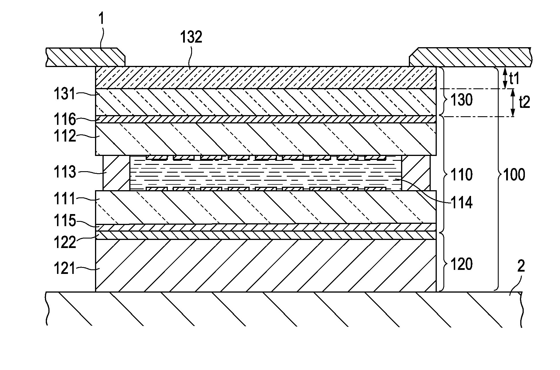
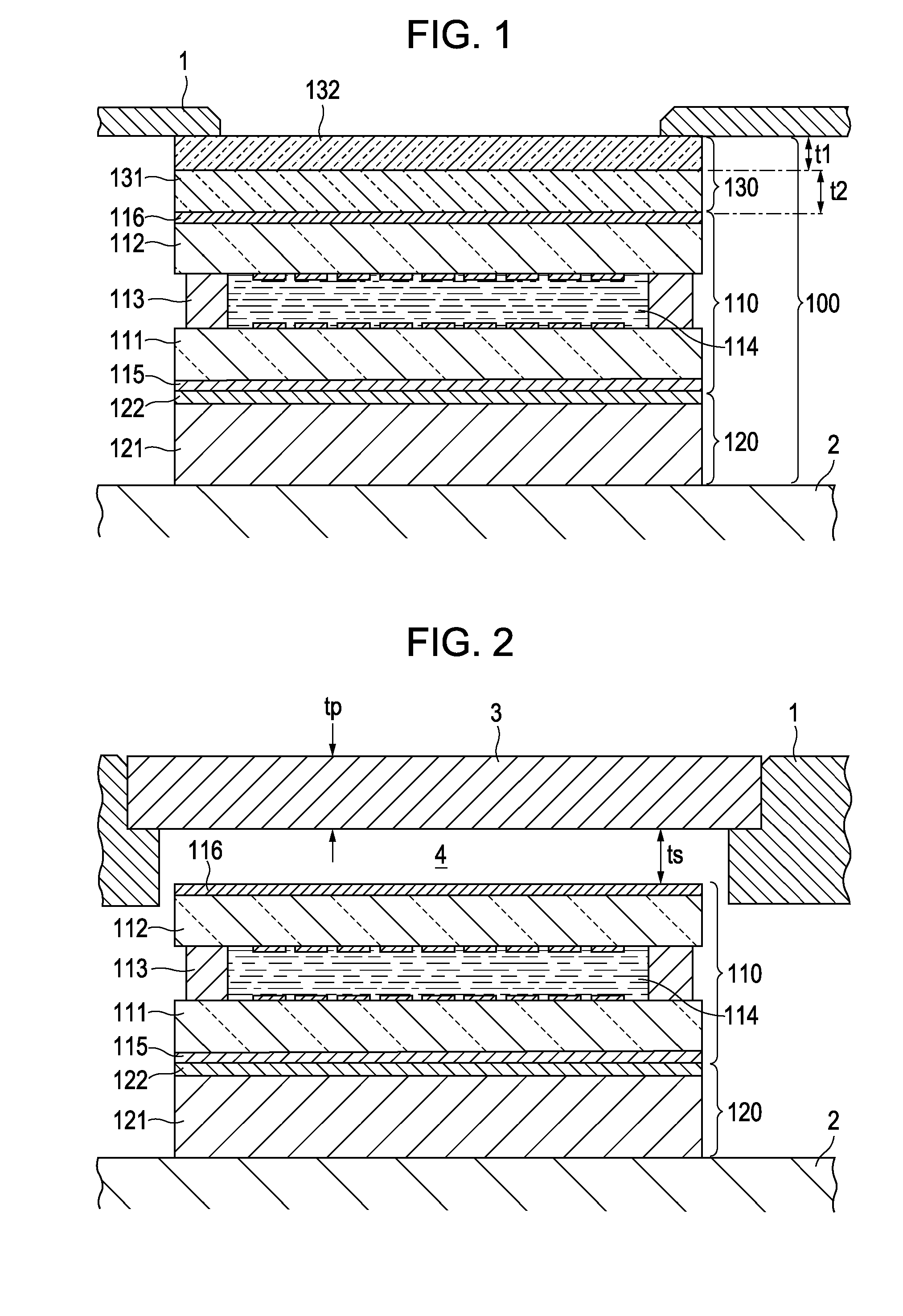
[0039] Hereinafter, embodiments of the invention will be described in detail with reference to the accompanying drawings. Firstly, an entire construction according to an embodiment of the invention will be described by exemplifying one of known constructions as a comparison example. FIG. 1 is a cross-sectional view schematically illustrating an electro-optical module according to an embodiment of the invention, which is installed in a chassis frame of an electronic device. FIG. 2 is a cross-sectional view schematically illustrating a state-of-the-art electro-optical module installed in a chassis frame of an electronic device as a comparison example.

[0040] Referring to FIG. 2 which shows a comparison example, an electro-optical module including a liquid crystal display panel 110 used as an electro-optical panel and an illumination unit 120 (such as a back-light unit) disposed at the rear of the liquid crystal display panel 110 is fixed on a board 2 installed in a chassis frame 1 of ...


PUM

PropertyMeasurementUnit
frequencyaaaaaaaaaa
thicknessaaaaaaaaaa
thicknessaaaaaaaaaa

Abstract

An electro-optical module includes: an electro-optical panel; and a transparent protector disposed on a viewer-side surface of the electro-optical panel, wherein transparent protector has a stack structure including a first transparent protection layer that faces the electro-optical panel and is formed of an elastic material and a second transparent protection layer that has a higher dynamic elasticity value than that of the first transparent protection layer within a frequency range of 1 to 10 Hz.

Description

[0001] This application claims the benefit of Japanese Patent Application No. 2005-247234, filed Aug. 29, 2005 and Japanese Patent Application No. 2006-147712, filed May 29, 2006. The entire disclosure of the prior applications is hereby incorporated by reference herein in its entirety. BACKGROUND [0002] 1. Technical Field [0003] The present invention relates to an electro-optical module and an electronic device, and more particularly, to a construction for improving impact resistance of an electro-optical module. [0004] 2. Related Art [0005] In general, electro-optical modules such as a liquid crystal display unit, an organic luminescence display unit, and a plasma display unit are widely used as a display module. These modules typically have a glass panel, a plastic panel, or the like. When these modules are externally impacted, the glass panel may be cracked, or the plastic panel may be deformed, and finally the display unit may be broken down. [0006] In a chassis frame of an ele...

Claims


Application Information

Patent Timeline
Patent Type & Authority Applications(United States)
IPC IPC(8): G02F1/1333
CPCG02F1/1333G02F1/133308Y10T428/1059Y10T428/1036G02F2001/133331C09K2323/03C09K2323/05G02F1/133331
Inventor SAKURAI, SHINJIIMASEKI, RYOSUKE
Owner JAPAN DISPLAY WEST
Why Eureka
Try Eureka