Non-volatile semiconductor memory device and method of manufacturing the same

a non-volatile semiconductor and memory device technology, applied in semiconductor devices, digital storage, instruments, etc., can solve the problems of overflowing electrical effect, increased difficulty in increasing the integration degree of non-volatile semiconductor memory devices, and improved coupling ratio, so as to achieve the effect of increasing the height of the floating gate pattern, suppressing or reducing cell disturbance, and increasing the integration degr

Inactive Publication Date: 2007-03-01
SAMSUNG ELECTRONICS CO LTD
View PDF8 Cites 50 Cited by
  • Summary
  • Abstract
  • Description
  • Claims
  • Application Information

AI Technical Summary

Benefits of technology

[0025] According to example embodiments, a line-shaped preliminary floating gate pattern may include a lower pattern having a first width and an upper pattern having a second width smaller than the first width so that a distance between the floating gate patterns adjacent to each other may increase and a cell disturbance between neighboring floating gate pattern

Problems solved by technology

However, the increased effective surface area of the floating gate may make it more difficult to increase an integration degree of the non-volatile semiconductor memory device because the space between the floating gate and adjacent other floating gate may be narrow.
As a result, a cell disturbance, may cause an overflowing electrical effect on neighboring cells adjacent to an operating cell corr

Method used


Image

  • Non-volatile semiconductor memory device and method of manufacturing the same
  • Non-volatile semiconductor memory device and method of manufacturing the same
  • Non-volatile semiconductor memory device and method of manufacturing the same

Examples


Embodiment Construction

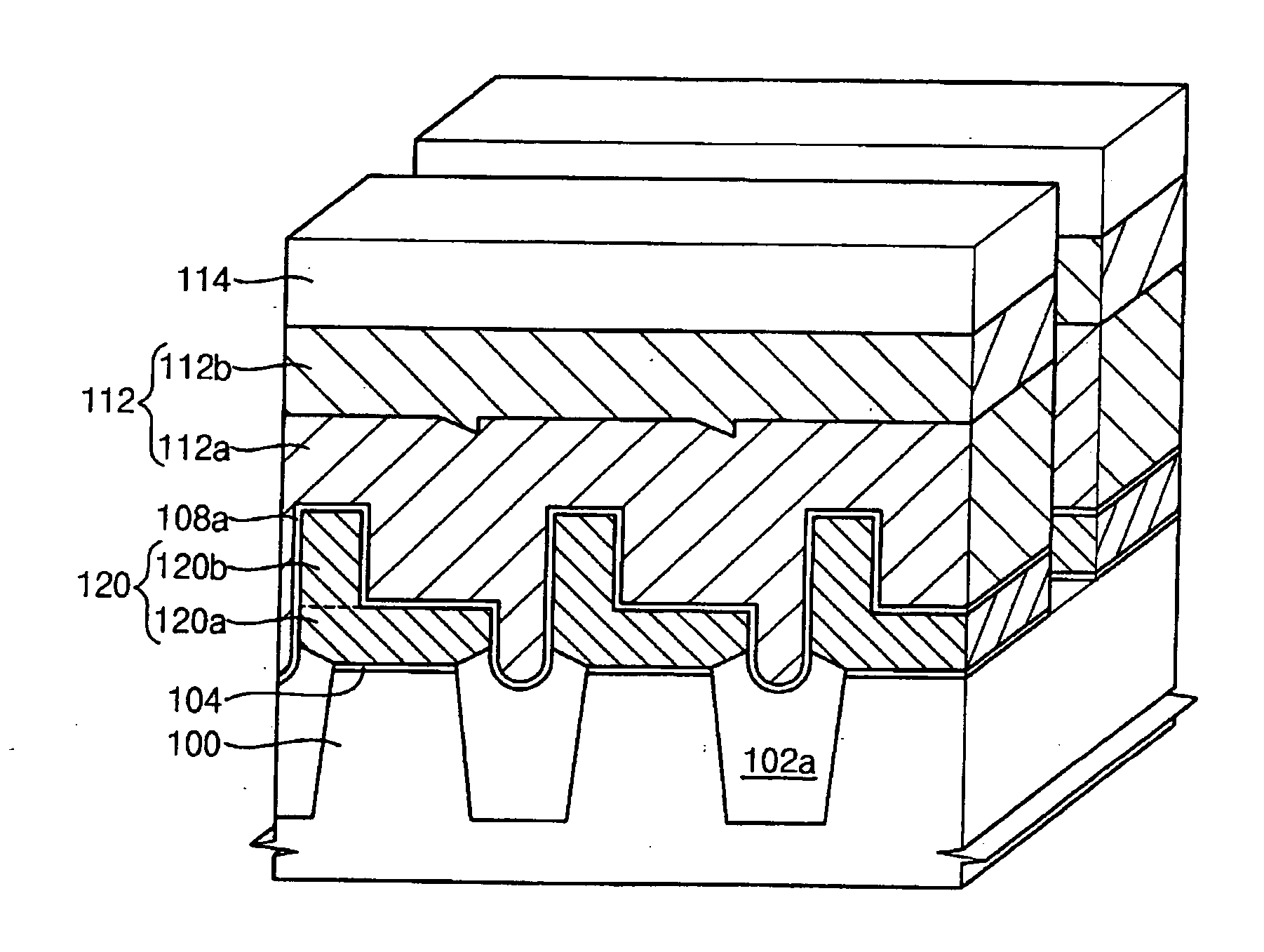
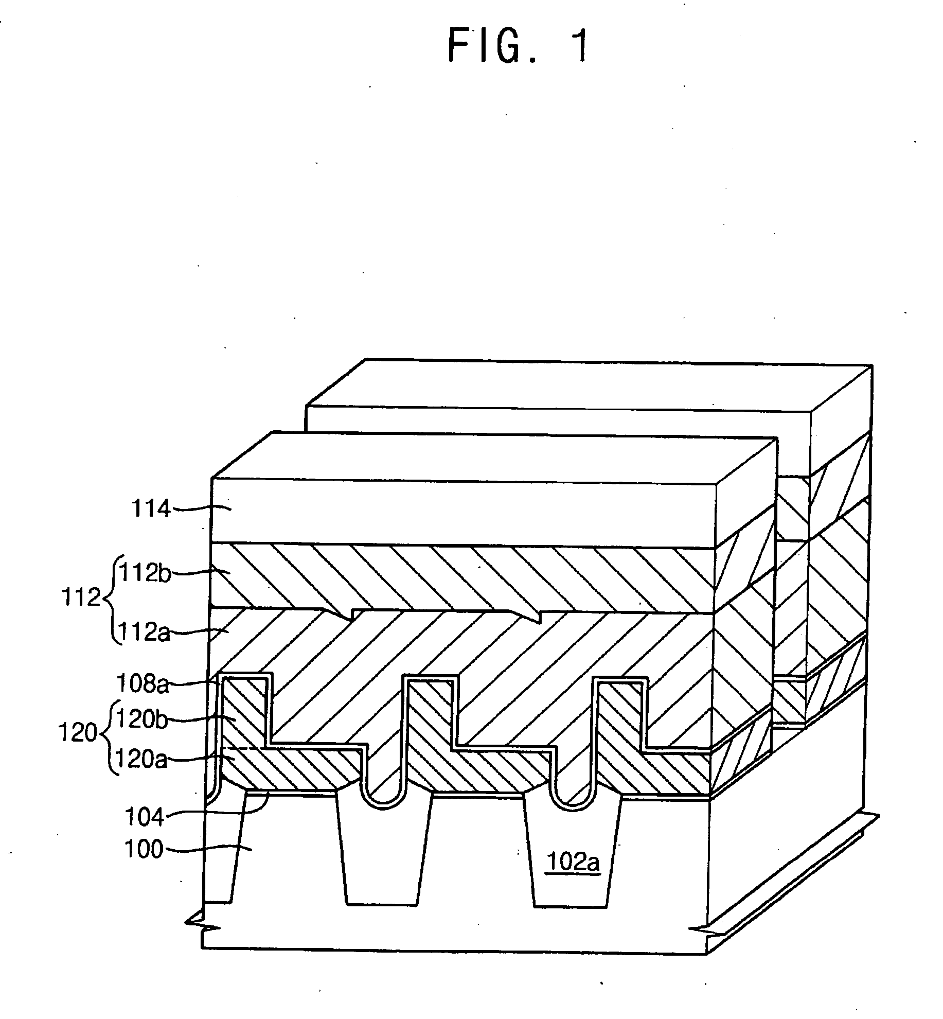
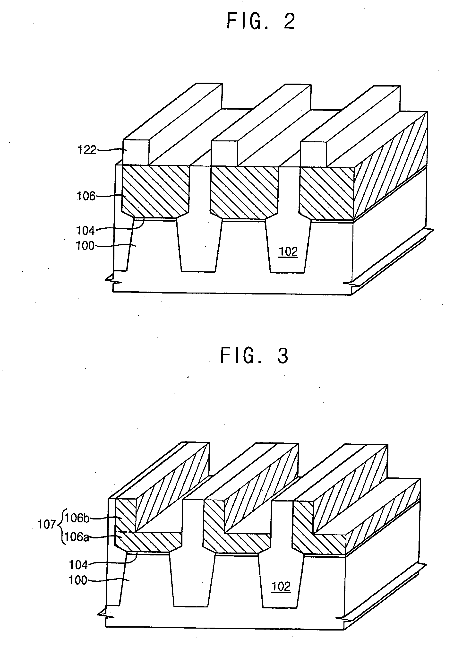
[0032] Hereinafter, example embodiments will be described in detail with reference to the accompanying drawings. It is understood that characteristics (e.g., thicknesses of layers, regions, etc.) illustrated in the drawings may be not drawn to scale. In the drawings, the sizes and relative sizes of layers and regions may be exaggerated for clarity.

[0033] Example embodiments are provided so that this disclosure will be thorough and complete, and will fully convey the scope of example embodiments to those skilled in the art. It will be understood that when an element or layer is referred to as being “on,”“connected to” or “coupled to” another element or layer, it can be directly on, connected or coupled to the other element or layer or intervening elements or layers may be present. In contrast, when an element is referred to as being “directly on,”“directly connected to” or “directly coupled to” another element or layer, there may be no intervening elements or layers present. Like nu...


PUM


Abstract

In a non-volatile memory device having a relatively high operation performance and a method of manufacturing the same, a substrate may be prepared to include an active region on which a conductive structure is located and defined by a field region in which an isolation layer is formed. A tunnel oxide layer may be formed on the active region of the substrate. A floating gate pattern may be formed on the tunnel oxide layer, and may include a lower part having a first width that is formed on the tunnel oxide layer and an upper part having a second width that is formed on the lower part, where the second width is substantially smaller than the first width. A dielectric layer pattern may be formed on the floating gate pattern, and a control gate pattern may be formed on the dielectric layer pattern. Accordingly, the non-volatile memory device may have an improved efficiency in programming and erasing data.

Description

PRIORITY CLAIM [0001] A claim of priority is made to Korean Patent Application No. 2005-80734 filed on Aug. 31, 2005, the contents of which may be herein incorporated by reference in their entirety. BACKGROUND [0002] 1. Field [0003] Example embodiments relate generally to a non-volatile semiconductor memory device and a method of manufacturing the non-volatile semiconductor memory device. For example, example embodiments relate to a non-volatile semiconductor memory device having an improved coupling ratio and a method of manufacturing the non-volatile semiconductor memory device having an improved coupling ratio. [0004] 2. Description of the Related Art [0005] A non-volatile semiconductor memory device is able to maintain data stored therein even when a power supply is cut off. For example, a flash memory device, one type of non-volatile semiconductor memory device, is capable of electrical programming or erasing stored data. [0006] A non-volatile semiconductor memory device may in...

Claims


Application Information

Patent Timeline
IPC IPC(8): G11C11/34
CPCH01L27/11521H01L27/115H10B69/00H10B41/30H01L21/823437H10B41/40
Inventor LEE, SEONG-SOOPARK, YOUNG-WOOKYIM, JANG-BINKIM, BUM-SUCHO, DU-HYUN
Owner SAMSUNG ELECTRONICS CO LTD
Why Eureka
Try Eureka