Non-Volatile Memory Device

a memory device and non-volatile technology, applied in static storage, digital storage, instruments, etc., can solve the problems of high possibility of cell state change, and high possibility of failure, and achieve the effect of reducing channel resistors and increasing cell curren

Active Publication Date: 2007-03-01
SK HYNIX INC
View PDF12 Cites 12 Cited by
  • Summary
  • Abstract
  • Description
  • Claims
  • Application Information

AI Technical Summary

Benefits of technology

[0016] A herein described embodiment increases a cell current by reducing channel resistors without

Problems solved by technology

Therefore, there is a high possibility that a cell state may be changed due to pass disturb in which erase cells are shallowly programmed.
In addition, even in non-selected strings, there i

Method used


Image

  • Non-Volatile Memory Device
  • Non-Volatile Memory Device
  • Non-Volatile Memory Device

Examples


Embodiment Construction

[0027] In the following detailed description, only certain exemplary embodiments of the present invention have been shown and described simply by way of illustration. As those skilled in the art will realize, the described embodiments may be modified in various different ways, all without departing from the spirit or scope of the present invention. Accordingly, the drawings and description are to be regarded as illustrative in nature and not restrictive. Like reference numerals designate like elements throughout.

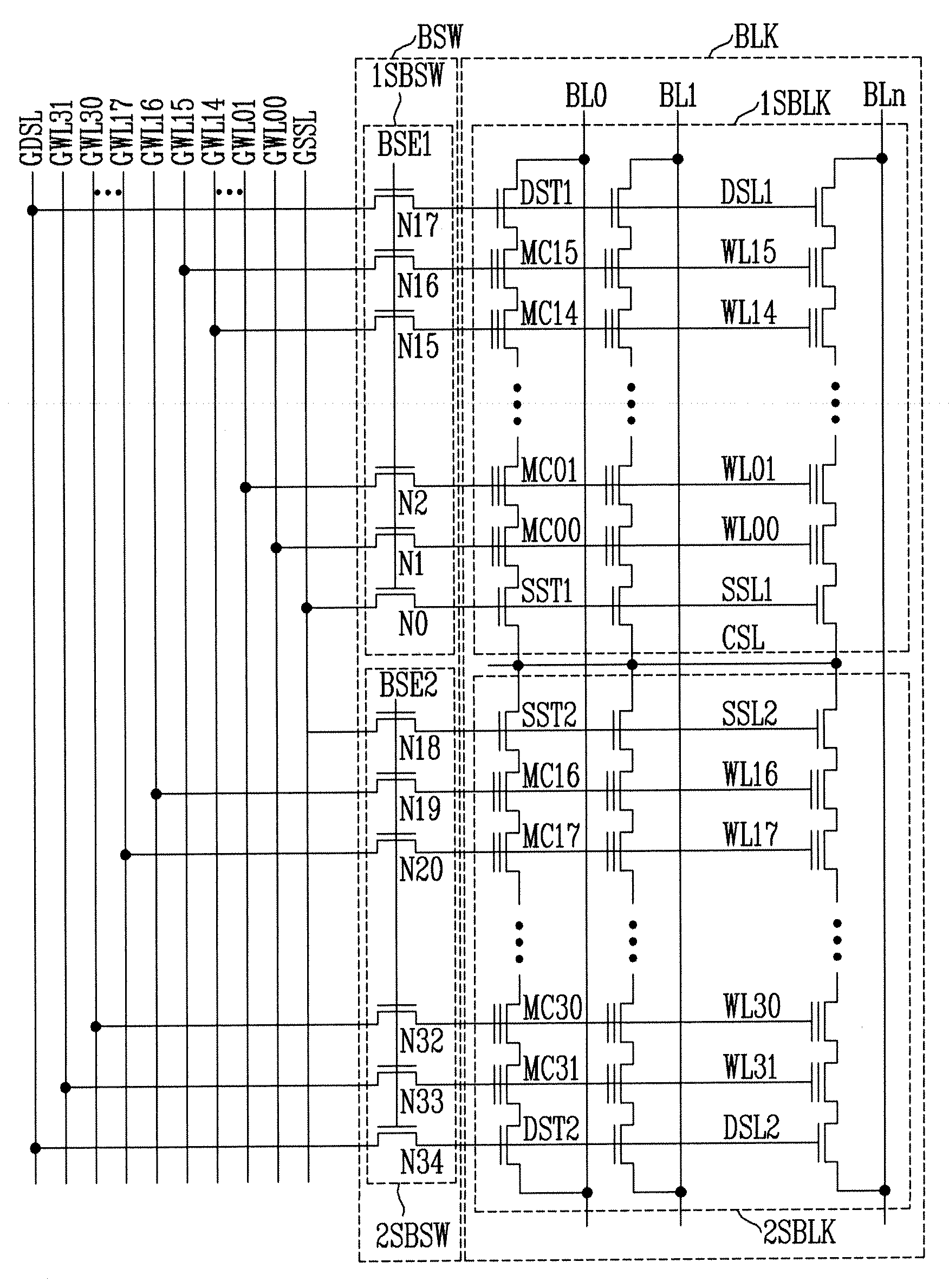
[0028]FIG. 4 is a block diagram of memory blocks of a non-volatile memory device.

[0029] Referring to FIG. 4, one completed memory block (for example, BLK0>) is divided into two sub memory blocks 1SBLK0>, 1SBLK0> unlike the related art. The reason why one block is divided into two sub memory blocks as described above is for reducing the cell current by reducing the number of channel resistor.

[0030] Basically, both the two sub memory blocks 1SBLK0>, 1SBLK0> within one memor...


PUM


Abstract

A non-volatile memory device may include a plurality of memory blocks including memory cells connected in series to bit lines, respectively. Each of the plurality of memory blocks may include a first sub memory block having a first group of memory cells, which are respectively connected in series between first select transistors connected to the bit lines, respectively, and second select transistors connected to a common source line, and a second sub memory block having a second group of memory cells, which are respectively connected in series between third select transistors connected to the bit lines, respectively, and fourth select transistors connected to the common source line.

Description

BACKGROUND [0001] 1. Technical Field [0002] This patent relates to non-volatile memory devices, and more particularly, to NAND flash memory devices in which one memory block is divided into two sub memory blocks. [0003] 2. Discussion of Related Art [0004] A flash memory is a kind of a non-volatile memory in which data can be stored even after power is turned off. The flash memory can be electrically programmed and erased and does not need the refresh function of rewriting data at regular intervals. The term “program” refers to the operation of programming data into the memory cells, and the term “erase” refers to the operation of erasing data from the memory cells. [0005] The flash memory device may be generally classified into NOR flash memory devices and NAND flash memory devices depending on the structure of the cell and operation conditions. In the NOR flash memory device, the source of each memory cell transistor is connected to the ground terminal (VSS) and program and erase f...

Claims


Application Information

Patent Timeline
IPC IPC(8): G11C8/00G11C11/34
CPCG11C16/24G11C16/0483G11C5/063G11C16/10G11C16/26
Inventor LEE, HEE YOUL
Owner SK HYNIX INC
Why Eureka
Try Eureka