

Clock and data recovery circuit
a clock and data recovery technology, applied in the field of circuits, can solve the problems of not performing the clock signal for edge detection and the control of the maximum segment of the respective phase shift of the clock signal for data sampling
- Summary
- Abstract
- Description
- Claims
- Application Information
AI Technical Summary
Benefits of technology
Problems solved by technology
Method used
Image

Examples
embodiment
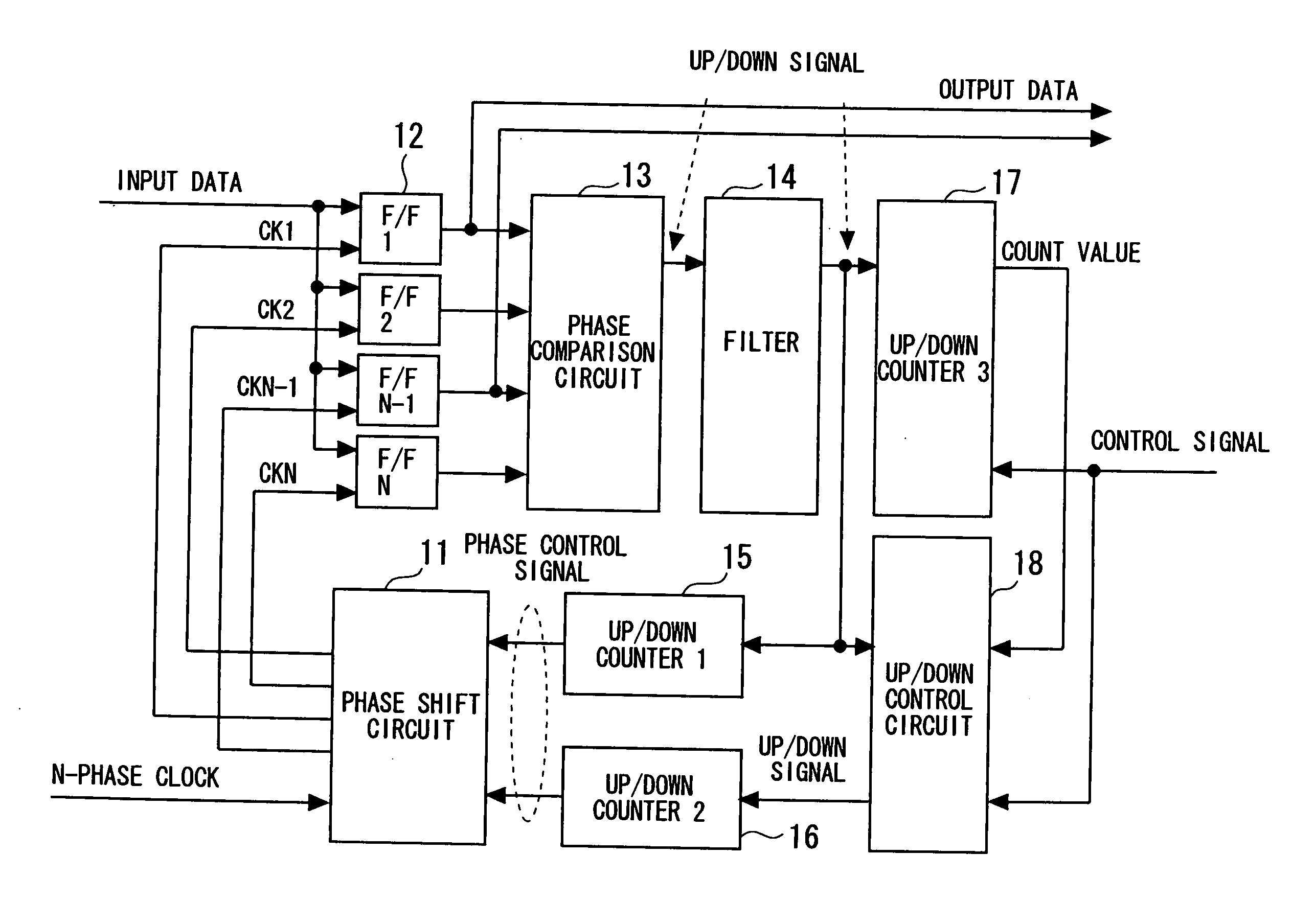
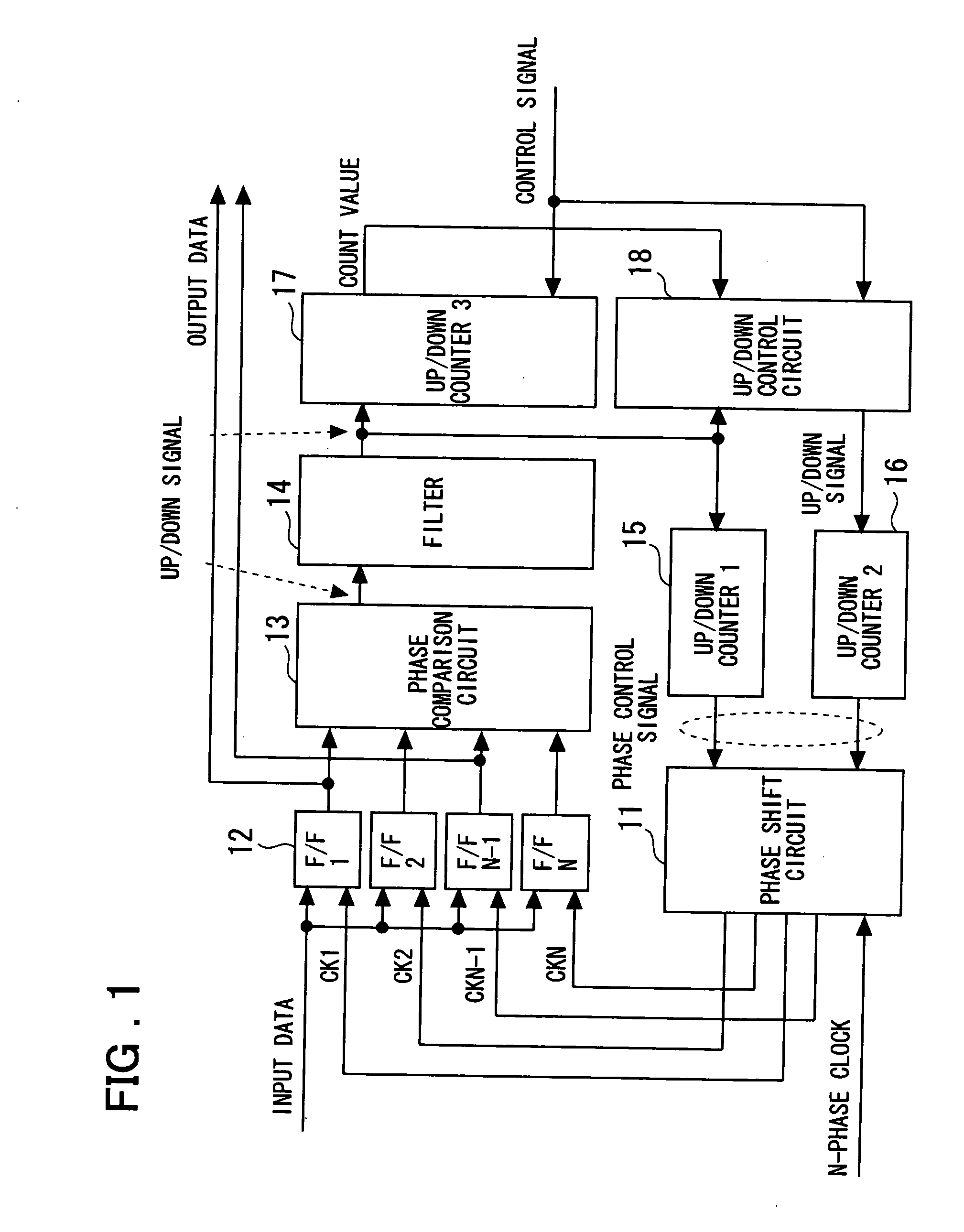
[0057]FIG. 1 is a diagram showing a configuration according to an embodiment of the present invention. Referring to FIG. 1, a clock and data recovery circuit according to the embodiment of the present invention receives an input data signal and includes N latch circuits 12 (constituted from flip-flops F / F1 to F / FN) for sampling the input data signal responsive to multiple phases of clock signals (constituted from N-phase clocks CK1 to CKN) from a phase shift circuit 11, respectively to output the sampled signals, a phase comparison circuit 13 for receiving outputs from the N latch circuits 12 (constituted from the F / F1 to F / FN), for phase comparison, and outputting an up / down signal based on a result of the comparison, a filter 14 for smoothing the up / down signal indicating the result of the comparison made by the phase comparison circuit 13, a first up / down counter 15 and a third up / down counter 17 each for receiving the up / down signal smoothed by the filter 14, and performing coun...
PUM
 Abstract
Description
Claims
Application Information