Stacked chip package using photosensitive polymer and manufacturing method thereof

a technology of photosensitive polymer and chip package, which is applied in the direction of semiconductor devices, semiconductor/solid-state device details, electrical apparatus, etc., can solve the problems of high yield, relative bulky and cumbersome modem applications, and difficulty in ensuring the quality of chips/wafers, so as to improve mechanical reliability, improve the adhesion between chips/wafers, and alleviate the problem of problems

Active Publication Date: 2007-03-01
SAMSUNG ELECTRONICS CO LTD
View PDF9 Cites 69 Cited by
  • Summary
  • Abstract
  • Description
  • Claims
  • Application Information

AI Technical Summary

Benefits of technology

[0010] The present invention provides for a stacked chip package configuration, and manufacturing methods thereof, wherein the gap between a lower and an upper chip is filled completely using a relatively simple process that eliminates voids, and the cracking and delamination problems associated with such voids. The present invention is applicable to both chip-level bonding and wafer-level bonding approaches. A photosensitive polymer layer is applied to a first chip, or wafer, prior to stacking the chips or stacking the wafers. The photosensitive polymer layer is partially cured, so that the photosensitive polymer layer is made to be structurally stable, while retaining its adhesive properties. The second chip, or wafer, is stacked, aligned, and bonded to the first chip, or wafer, and the photosensitive polymer layer is then cured to fully bond the first and second chips, or wafers. In this manner, adhesion between chips / wafers is greatly improved, while providing complete fill of the gap. In addition, mechanical reliability is improved, alleviating the problems associated with cracking and delamination. This leads to an improvement in device yield and device reliability.

Problems solved by technology

The resulting MSPs enjoyed widespread use in the past, but are relatively bulky and cumbersome for modem applications.
The resulting MCPs have characteristically high yield, however, process throughput is a problem, as each individual chip needs to be handled during alignment and bonding processes.
The resulting WL CSPs suffer from low yield.
Chip level bonding and wafer level bonding are generally complicated and unstable manufacturing processes.
The underfill process is unreliable, since the gap between the lower and upper chip substrates is small, for example on the order of 20 μm.
If the underfill process does not result in a complete and uniform fill of the gap, then any resulting voids can increase the likelihood of future generation of cracks.
Such cracks can propagate during future heating and cooling cycles, decreasing the reliability of the resulting chip stack device.
Such stress is typically caused by a mismatch in coefficient of thermal expansion (CTE) between two adjacent layers.
Such CTE mismatch can cause further cracking and delamination when subjected to numerous heating and cooling thermal cycles, negatively affecting device yield during manufacture, and device reliability during operation.

Method used


Image

  • Stacked chip package using photosensitive polymer and manufacturing method thereof
  • Stacked chip package using photosensitive polymer and manufacturing method thereof
  • Stacked chip package using photosensitive polymer and manufacturing method thereof

Examples


Embodiment Construction

[0055] The present invention will now be described more fully hereinafter with reference to the accompanying drawings, in which preferred embodiments of the invention are shown. This invention may, however, be embodied in different forms and should not be construed as limited to the embodiments set forth herein. In the drawings and related description, if a first layer is referred to as being “on” another layer, the first layer can be directly on the other layer, or intervening layers may be present. Like numbers refer to like elements throughout the specification.

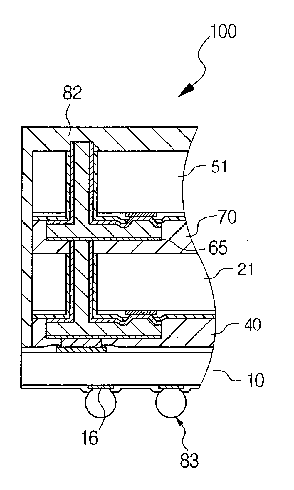
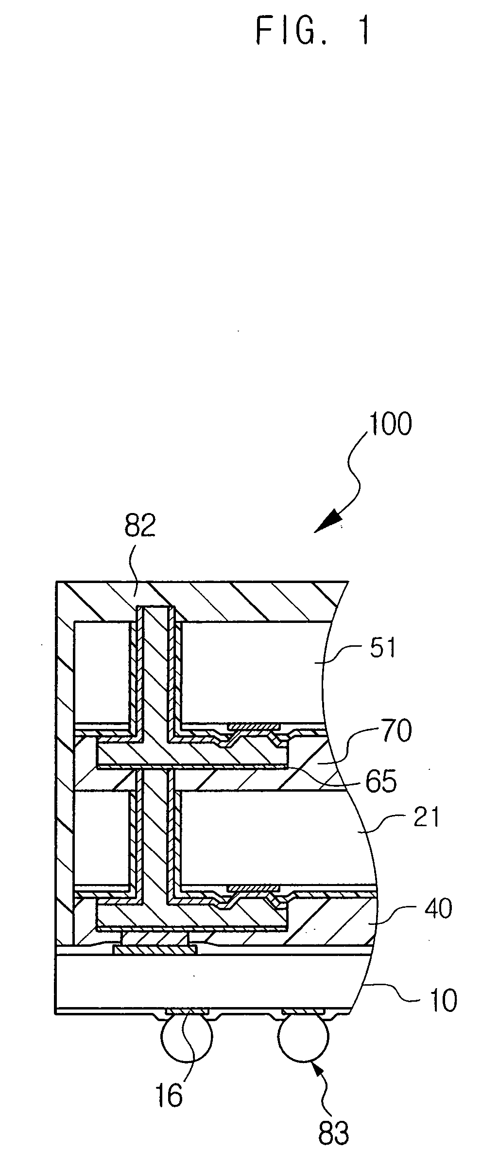
[0056]FIG. 1 is a sectional view of a stacked chip package in accordance with the present invention. A stacked chip package according to the embodiment of FIG. 1 includes a printed. circuit board 10, upon which a chip stack including a first chip 21 and a second chip 51 are mounted. The first chip 21 is mechanically bonded to the printed circuit board 10 by a first photosensitive polymer layer 40. The second chip 51 is me...


PUM


Abstract

In a stacked chip configuration, and manufacturing methods thereof, the gap between a lower and an upper chip is filled completely using a relatively simple process that eliminates voids between the lower and upper chips and the cracking and delamination problems associated with such voids. The present invention is applicable to both chip-level bonding and wafer-level bonding approaches. A photosensitive polymer layer is applied to a first chip, or wafer, prior to stacking the chips or stacking the wafers. The photosensitive polymer layer is partially cured, so that the photosensitive polymer layer is made to be structurally stable, while retaining its adhesive properties. The second chip, or wafer, is stacked, aligned, and bonded to the first chip, or wafer, and the photosensitive polymer layer is then cured to fully bond the first and second chips, or wafers. In this manner, adhesion between chips/wafers is greatly improved, while providing complete gap fill. In addition, mechanical reliability is improved, alleviating the problems associated with cracking and delamination, and leading to an improvement in device yield and device reliability.

Description

RELATED APPLICATIONS [0001] This application claims priority under 35 U.S.C. 119 to Korean Patent Application No. 10-2005-0080655 filed on Aug. 31, 2005, the content of which is incorporated herein by reference in its entirety. This application is related to United States Patent Application Serial No. ______, entitled “Stacked Chip Package Using Warp Buffer Insulative Material and Manufacturing Method Thereof”, by Yong-Chai Kwon, et al., filed of even date herewith and commonly owned with the present application, the content of which is incorporated herein by reference in its entirety. FIELD OF THE INVENTION [0002] The present invention relates to semiconductor device packages including a stacked chip package configuration that utilizes a photosensitive polymer, and manufacturing methods thereof. BACKGROUND OF THE INVENTION [0003] Semiconductor manufacturing and packaging technology has evolved to the point where device packages can include multiple integrated circuit chips that are...

Claims


Application Information

Patent Timeline
Patent Type & Authority Applications(United States)
IPC IPC(8): H01L21/30
CPCH01L21/76898H01L23/481H01L2924/0002H01L2224/0401H01L2924/0665H01L2924/014H01L2924/0105H01L2924/01033H01L2924/01024H01L2924/01006H01L24/11H01L24/12H01L24/16H01L24/31H01L24/83H01L24/90H01L24/94H01L25/0657H01L25/50H01L2221/68372H01L2224/02311H01L2224/02321H01L2224/0557H01L2224/13009H01L2224/13021H01L2224/13099H01L2224/16145H01L2224/83136H01L2224/83194H01L2224/838H01L2225/06513H01L2225/06524H01L2225/06541H01L2924/01013H01L2924/01022H01L2924/01029H01L2924/01046H01L2924/01073H01L2924/01075H01L2924/01079H01L2924/01082H01L2924/01322H01L2924/04953H01L2924/14H01L2224/16147H01L2224/16237H01L2224/81141H01L2224/2919H01L2924/01005H01L2924/00H01L2924/3512H01L2224/05552H01L24/02H01L24/13H01L2224/02372H01L2224/02379H01L2224/05568H01L2224/05571H01L2224/08112H01L2224/16148H01L2924/0001H01L2924/181H01L2224/02H01L23/12H01L23/48
Inventor KWON, YONG-CHAILEE, KANG-WOOKMA, KEUM-HEEHAN, SEONG-II
Owner SAMSUNG ELECTRONICS CO LTD
Why Eureka
Try Eureka