Semiconductor device

Inactive Publication Date: 2007-03-08
NEC ELECTRONICS CORP
View PDF3 Cites 22 Cited by
  • Summary
  • Abstract
  • Description
  • Claims
  • Application Information

AI Technical Summary

Problems solved by technology

In this point of view, the configuration in the region corresponded to the boundary region described in the Japan...

Method used


Image

  • Semiconductor device
  • Semiconductor device
  • Semiconductor device

Examples


Embodiment Construction

[0032] The invention will be now described herein with reference to an illustrative embodiment. Those skilled in the art will recognize that many alternative embodiments can be accomplished using the teachings of the present invention and that the invention is not limited to the embodiment illustrated for explanatory purposes.

[0033] Paragraphs below will describe embodiments of the present invention referring to the attached drawings.

[0034] It is to be noted that any common constituents will be given with the same reference numerals, and the explanation will not be repeated. The embodiment below deals with the case where the first conductivity type is n-type, and the second conductivity type is p-type.

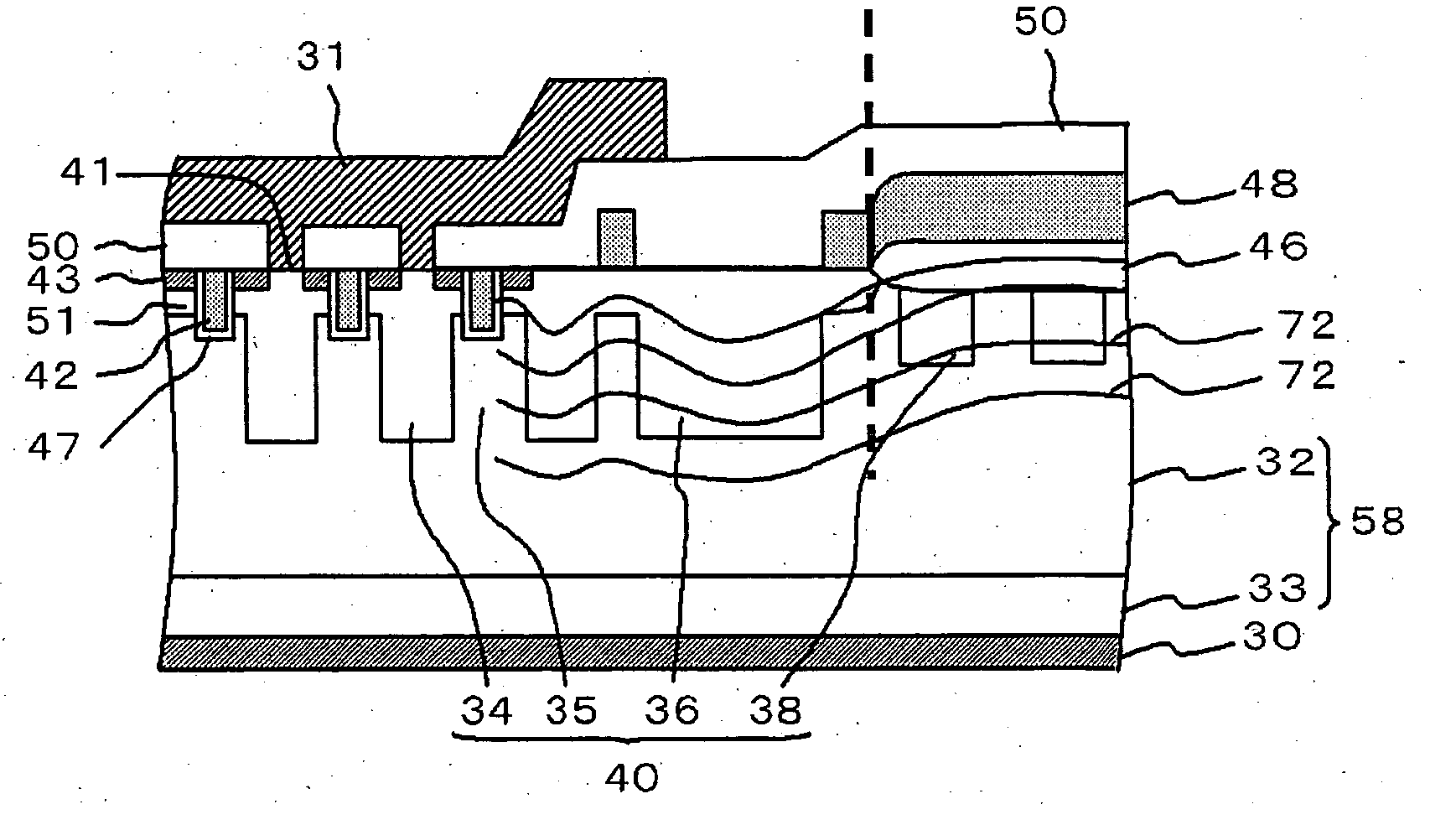
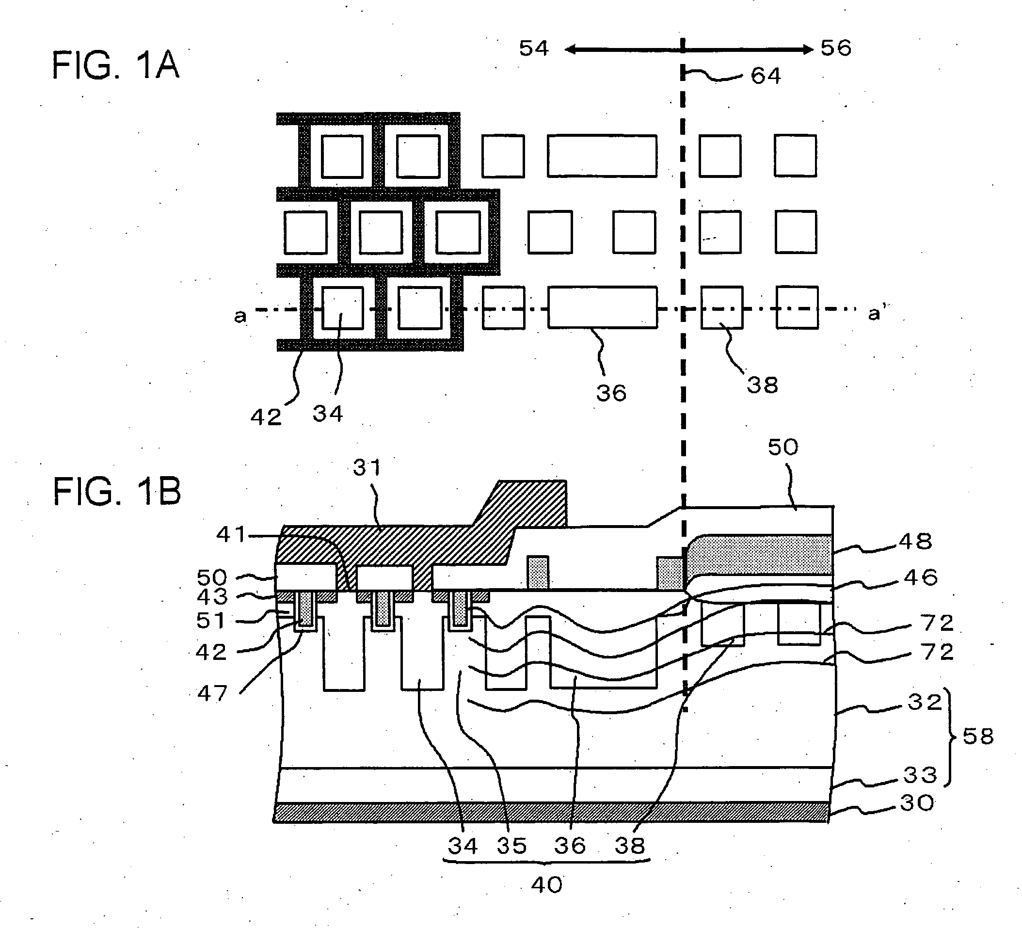
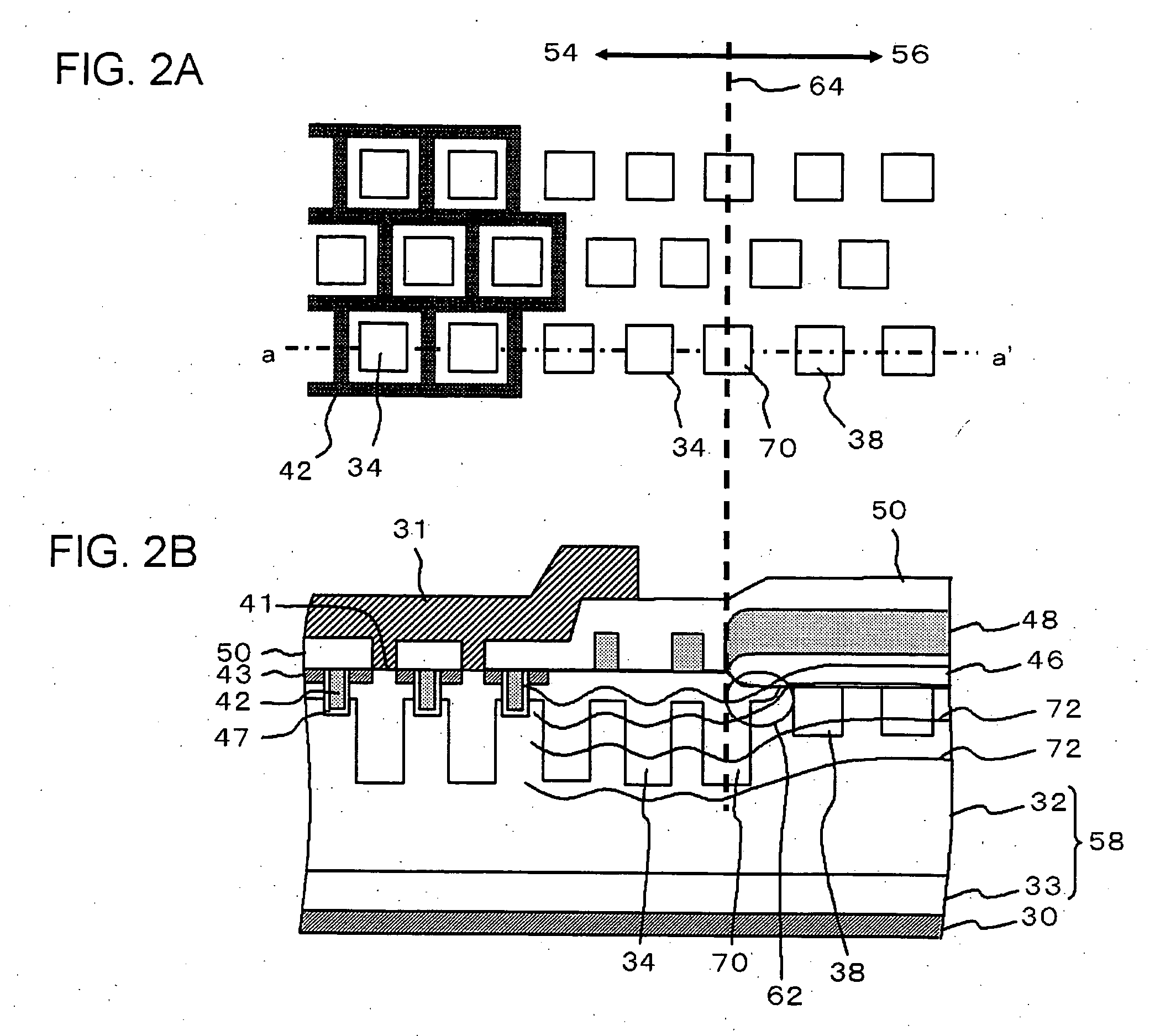
[0035]FIG. 1A is a top view showing a configuration of the outermost region of a semiconductor device according to one embodiment, and FIG. 1B is a sectional view taken along line a-a′ in FIG. 1A.

[0036]FIG. 1B is a sectional view showing a configuration of the semiconductor device ...


PUM


Abstract

Aiming at realizing high breakdown voltage and low ON resistance of a semiconductor device having the super-junction structure, the semiconductor device of the present invention has a semiconductor substrate having an element forming region having a gate electrode formed therein, and a periphery region formed around the element forming region, and having an field oxide film formed therein; and a parallel p-n layer having n-type drift regions and p-type column regions alternately arranged therein, formed along the main surface of the semiconductor substrate, as being distributed over the element forming region and a part of the periphery region, wherein the periphery region has no column region formed beneath the end portion on the element forming region side of the field oxide film and has p-type column regions as at least one column region formed under the field oxide film.

Description

[0001] This application is based on Japanese patent applications No. 2005-258747 and No. 2006-122976 the contents of which are incorporated hereinto by reference. DISCLOSURE OF THE INVENTION [0002] 1. Field of the Invention [0003] The present invention relates to a semiconductor device, and in particular to a semiconductor device having the super-junction structure. [0004] 2. Related Art [0005] Vertical power MOSFET has been proposed as a high-voltage-type MOS field effect transistor (MOSFET). Critical characteristics of this sort of high-voltage MOSFET include ON-resistance and breakdown voltage. The ON-resistance and the breakdown voltage depend on resistivity of an electric field moderating layer, wherein a trade-off relation resides in that lowering in the resistivity by raising the impurity concentration of the electric field moderating layer successfully results in reduction in the ON-resistance, but also in lowering in the breakdown voltage at the same time. [0006] In recent ...

Claims


Application Information

Patent Timeline
IPC IPC(8): H01L29/76
CPCH01L29/0634H01L29/0696H01L29/1095H01L29/7813H01L29/66734H01L29/7811H01L29/402
Inventor MIURA, YOSHINAONINOMIYA, HITOSHI
Owner NEC ELECTRONICS CORP
Why Eureka
Try Eureka