

Method and Schottky diode structure for avoiding intrinsic NPM transistor operation
a technology diode structure, which is applied in the direction of diodes, semiconductor devices, electrical apparatus, etc., can solve the problems of large unusable effectiveness of parasitic devices and not being used much, and achieve the effect of avoiding undesired operation of intrinsic bipolar transistor structures
- Summary
- Abstract
- Description
- Claims
- Application Information
AI Technical Summary
Benefits of technology
Problems solved by technology
Method used
Image

Examples
Embodiment Construction
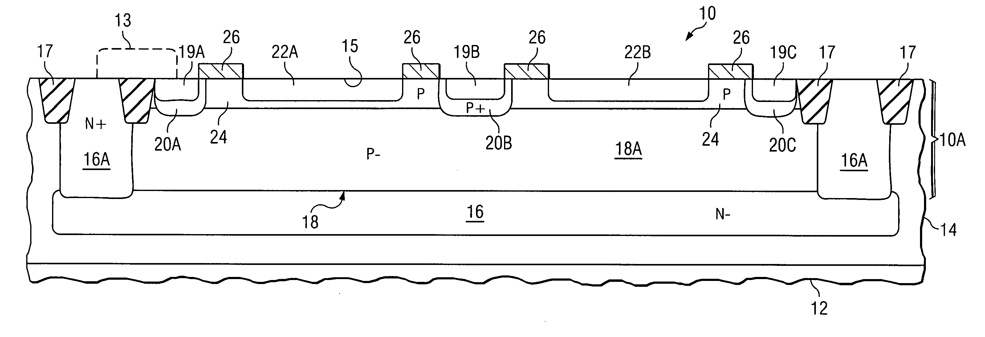
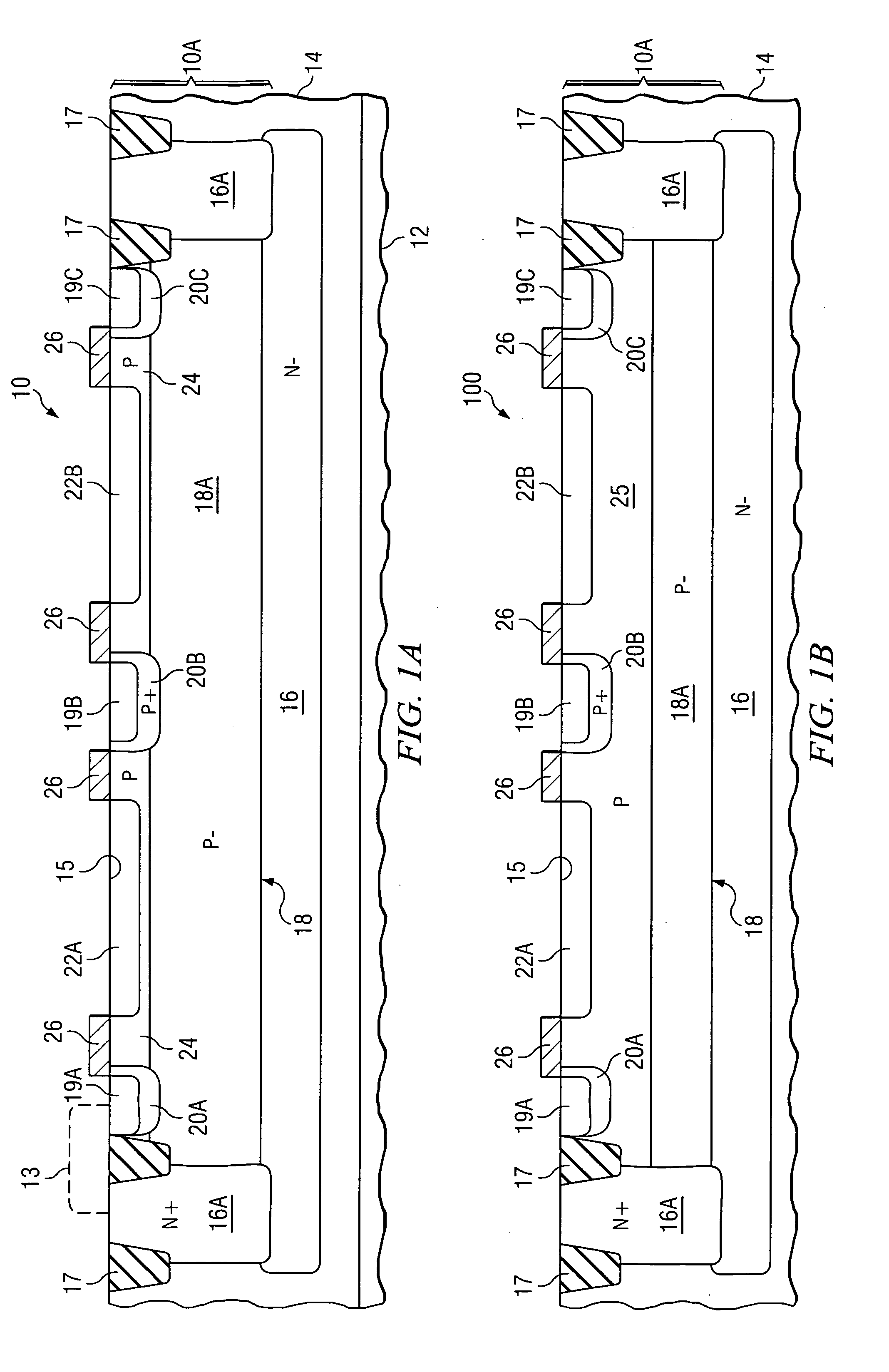
[0028] Referring to FIG. 1A, integrated circuit lateral Schottky diode structure 10 includes a lightly doped P-type region 14 formed on a wafer substrate 12. A lightly doped N-type well region 16 is formed in P-type region 14, which can be, but does not need to be, an epitaxial silicon layer formed on a wafer 12. After formation of a deep N-well region using a very high energy (MeV) implantation, a lightly doped P-type region 18, including a deep “bulk” portion thereof, remains over the buried—well region 16. A closed N+ sidewall isolation region 16A surrounds the sides of P-type region 18 and extends downward from the upper surface of integrated circuit structure 10 into the upper surface of N-well region 16. A STI (shallow trench region isolation) trench 17 is formed along the inner and outer upper surface edges of closed N+ sidewall isolation region 16A. The P− anode bulk region 18A forms an anode region of a lateral Schottky diode 10A. The P+ anode contact regions 20A, 20B and 2...
PUM
 Abstract
Description
Claims
Application Information