Eureka AIR delivers breakthrough ideas for toughest innovation challenges, trusted by R&D personnel around the world.

Metal line for a semiconductor device and fabrication method thereof

Inactive Publication Date: 2007-03-08
DONGBU ELECTRONICS CO LTD
View PDF9 Cites 7 Cited by
  • Summary
  • Abstract
  • Description
  • Claims
  • Application Information

AI Technical Summary

Benefits of technology

[0033] An advantage of the present invention is that it provides a metal line for a semiconductor device which can be used in a semiconductor device structure less than 65 nm deep using CVC TiSiN as a material for a barrier metal layer, and a fabrication method thereof.
[0034] Additional advantages and features on the invention will be set forth in the description which follows, and in part will be apparent from the description, or may be learned by practice of the invention. These and other advantages of the invention will be realized and attained by the structure particularly pointed out in the written description and claims hereof as well as the appended drawings.
[0035] To achieve these and other advantages and in accordance with the purpose of the present invention, as embodied and broadly described, a metal line for a semiconductor device comprising: a semiconductor substrate having a semiconductor device formed thereon; an insulating layer which has a contact hole at a portion corresponding to the semiconductor device and is formed on the semiconductor substrate; a TiSiN barrier metal layer which is formed in the contact hole; and a copper line which is formed on the TiSiN barrier metal layer.
[0036] According to another aspect of the present invention, a metal line for a semiconductor device comprises a semiconductor substrate having a semiconductor device formed thereon; an insulating layer which has a contact hold at a portion corresponding to the semiconductor device is formed on the semiconductor substrate; a barrier metal layer which consists of a TiSiN layer formed in the contact hold and a Ta layer laminated on the TiSiN; and a copper line which is formed on the barrier metal layer.
[0037] According to another aspect of the present invention, a method of fabricating a metal line for a semiconductor device comprising steps of: forming a semiconductor device on a semiconductor substrate; forming a contact hole at a portion corresponding to the semiconductor device by depositing an insulating layer on the semiconductor substrate and selectively removing the insulating layer; forming a TiSiN barrier metal layer formed on the whole surface of the semiconductor substrate including the contact hole; forming a copper layer on the TiSiN barrier metal layer; and grinding the copper layer and the TiSiN barrier metal layer to expose the surface of the insulating layer.
[0038] In the aforementioned aspect of the method, the step of forming the TiSiN barrier metal layer may further comprise: a first step of depositing a thermal TiN layer using a tetrakis dimethyl amino titanium (TDMAT) material; a second step of forming a CVD nitride titanium (TiN) layer by performing a plasma process on the thermal TiN; and a third step of forming a CVD TiSiN layer by reacting SiH4 gas with the CVD TiN layer.

Problems solved by technology

However, since the Al has a relatively high resistivity, it has been known that the Al is not an appropriate metal for lines in ultra large scale integration (ULSI) and giga scale integration (GSI).
However, when using copper, dry etching cannot not be easily performed, copper's adhesion characteristic with respect to a silicon oxide layer (SiO2) is not good, and the thermodynamic stability and corrosion resistance of copper are low.
Furthermore, copper rapidly diffuses in silicon (Si) and SiO2 and generates a leakage current in a pn-junction by forming a deep donor level in the Si, causing a malfunction of the semiconductor device.
However, when the barrier metal is deposited to a thickness greater than 100 Angstroms by sputtering in a semiconductor device structure that is less than 65 nm in size, an overhang is inevitably created at the upper side of the via or trench.
Thus, a problem such as void may occur in integrating with the copper.
As a result, a barrier metal formation using the sputtering method is limited to semiconductor device structures that are 65 nm in size or larger.
First, as mentioned above, since the barrier metal layer is formed using a PVD method, the barrier metal layer is not uniformly deposited.
Second, since the barrier metal layer is formed using a PVD method, it is difficult to deposit a barrier metal layer that is less than 100 Angstroms thick.
Thus, it cannot be used in a semiconductor device structure that is less than 65 nm in size.

Method used


Image

  • Metal line for a semiconductor device and fabrication method thereof
  • Metal line for a semiconductor device and fabrication method thereof
  • Metal line for a semiconductor device and fabrication method thereof

Examples


Embodiment Construction

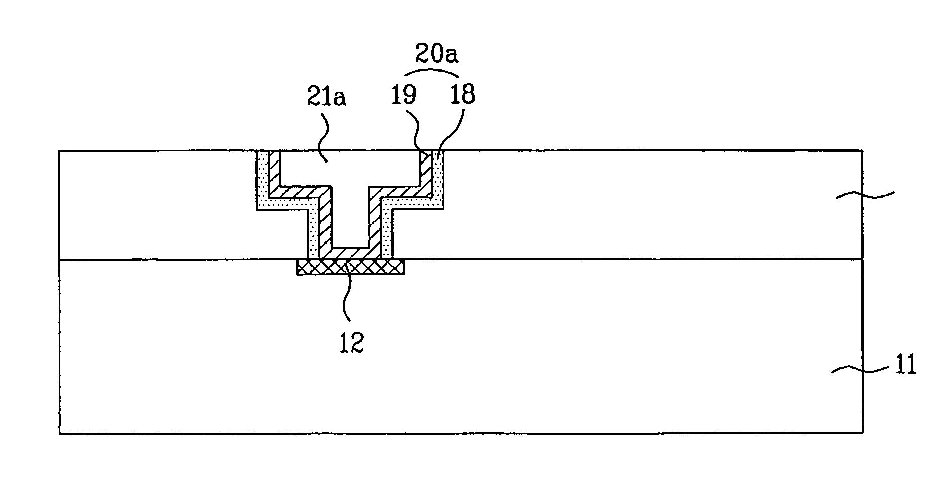
[0052] Reference will now be made in detail to exemplary embodiments of the present invention, examples of which are illustrated in the accompanying drawings.

[0053]FIGS. 2A to 2D are sectional views of a semiconductor device fabricated with a process of forming a copper line in accordance with an exemplary embodiment of the present invention.

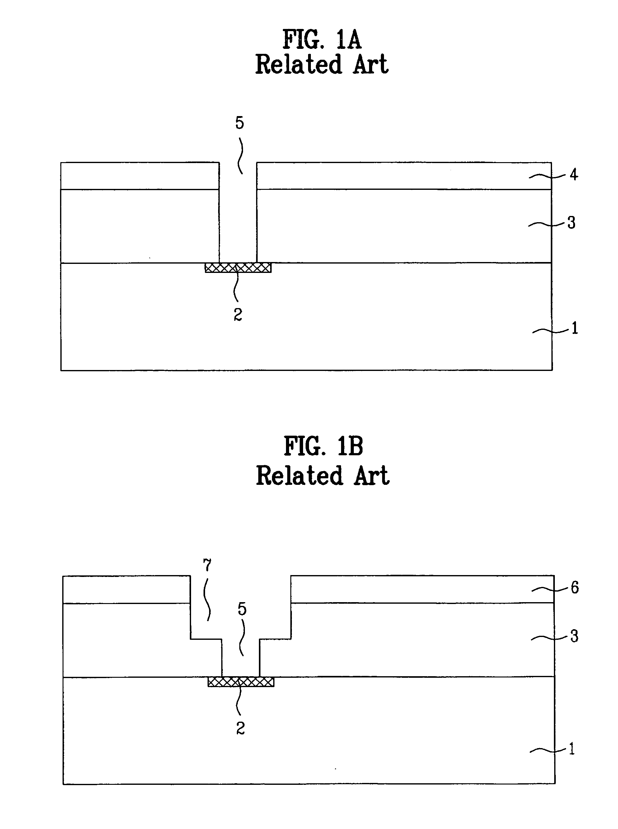
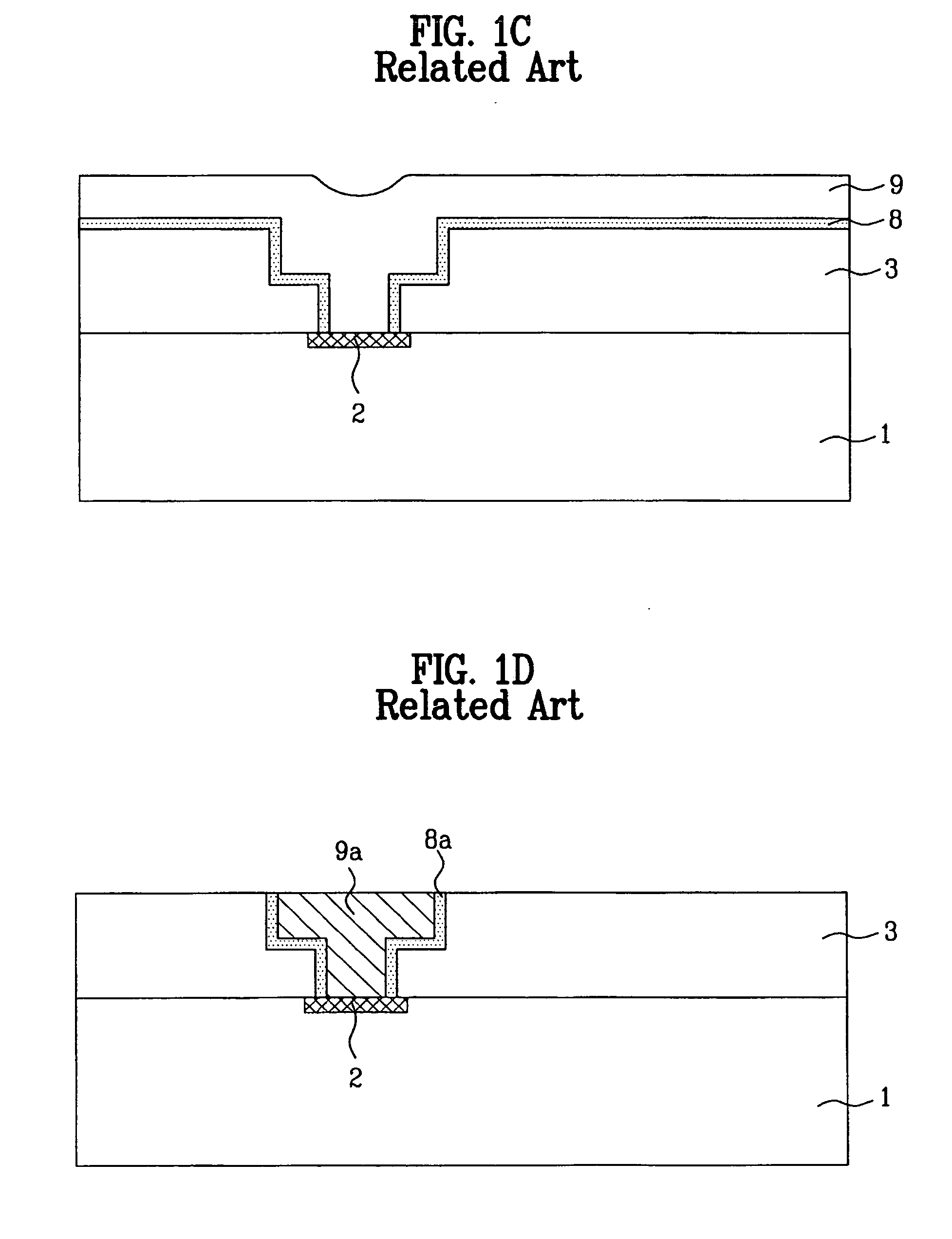
[0054] As shown in FIG. 2A, impurity ions are implanted in a semiconductor substrate 11 to form a semiconductor device 12.

[0055] Next, an insulating layer 13 such as a nitride oxide layer, an oxide layer, FSG, or BPSG is formed on the whole surface of the semiconductor substrate 11 including the semiconductor device 12.

[0056] A first photoresist 14 is coated on the insulating layer 13, and a contact area is then defined by patterning the first photoresist 14 by exposing or developing processes.

[0057] Next, a contact hole 15 is formed by selectively removing the insulating layer 13 using the patterned first photoresist 14 as a mask.

[0058] A...


PUM


Abstract

A metal line, which can be used in a semiconductor device structure less than 65 nm in size by forming a barrier metal of an anti-diffusion layer for a copper line using CVD TiSiN, and a fabrication method thereof are provided. The metal line includes: a semiconductor substrate having a semiconductor device formed thereon; an insulating layer which has a contact hole at a portion corresponding to the semiconductor device and is formed on the semiconductor substrate; a TiSiN barrier metal layer which is formed in the contact hole; and a copper line which is formed on the TiSiN barrier metal layer.

Description

CROSS REFERENCE TO RELATED APPLICATIONS [0001] This application claims the benefit of the Korean Patent Application No. P2005-0079507, filed on Aug. 29, 2005, which is hereby incorporated by reference as if fully set forth herein. BACKGROUND OF THE INVENTION [0002] 1. Field of the Invention [0003] The present invention relates to a copper line for a semiconductor device, and more particularly, to a metal line for a semiconductor device in which a barrier metal used as an anti-diffusion layer for the copper line is formed using CVD TiSiN, and a fabrication method thereof. [0004] 2. Description of the Related Art [0005] As the size of semiconductor devices has recently decreased, the line width and thickness of a metal line for a semiconductor device has also decreased. To cope with the reduction of the line width and thickness of the semiconductor device, aluminum (Al) has been widely used as a material for the metal line. [0006] However, since the Al has a relatively high resistivit...

Claims


Application Information

Patent Timeline
IPC IPC(8): H01L23/52H01L21/4763
CPCH01L21/28556H01L21/76843H01L21/76844H01L21/76846H01L2924/0002H01L23/53238H01L2924/00H01L21/28
Inventor JOO, SUNG JOONGLEE, HAN CHOON
Owner DONGBU ELECTRONICS CO LTD
Why Eureka
Eureka Blog
Learn More