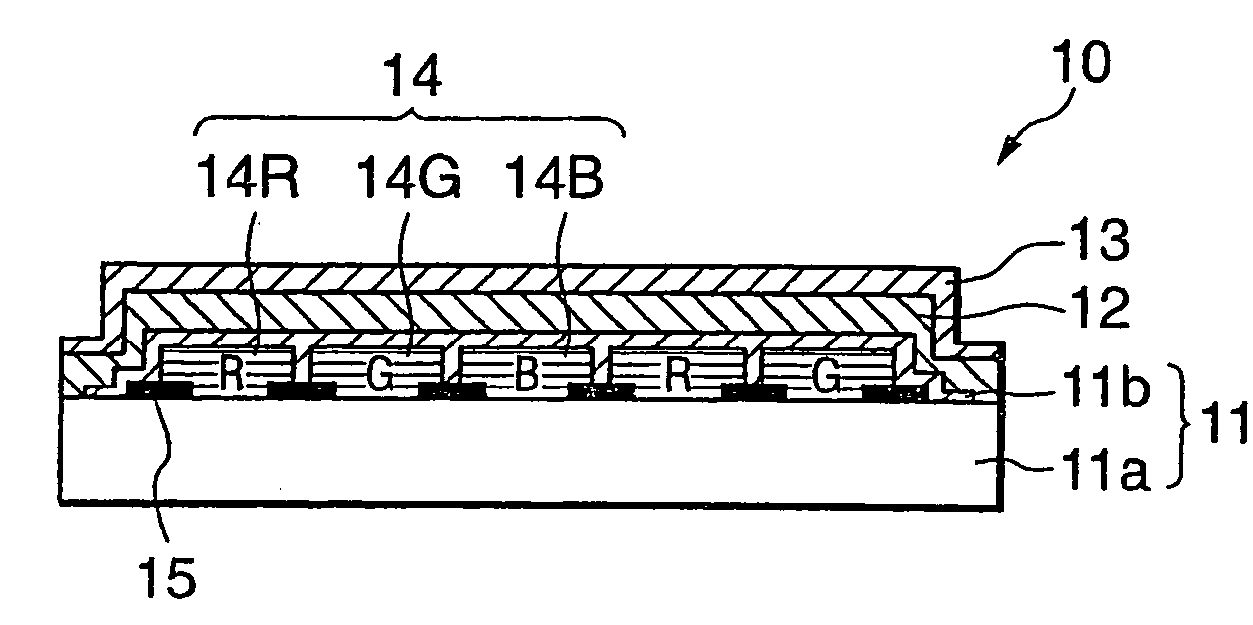
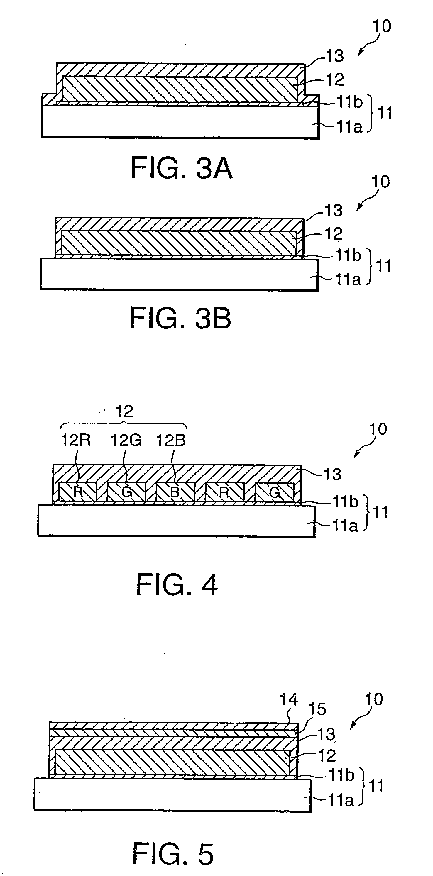
Optical element

a technology of optical elements and liquid crystals, applied in the field of optical elements, can solve the problems of large increase in power consumption, low optical efficiency of conventional liquid crystal display, and high hardness of parts, and achieve the effects of high hardness, high display quality, and deterioration of liquid crystal layers

Active Publication Date: 2007-03-08
DAI NIPPON PRINTING CO LTD
View PDF9 Cites 2 Cited by
  • Summary
  • Abstract
  • Description
  • Claims
  • Application Information

AI Technical Summary

Benefits of technology

[0011] The present invention was accomplished in the light of the aforementioned drawbacks in the related art. An object of the present invention is to provide a high-quality optical element including a liquid crystal layer, having the advantages that the film thickness distribution of the liquid crystal layer remains uniform even when forces are externally exerted to the optical element in the process of production of the optical element or in the course of incorporation of the optical element in a liquid crystal display, and that the optical element can maintain its high displaying quality even when incorporated in a liquid crystal display.
[0019] In the present invention, on top of the liquid crystal layer made by forming and curing a film of a liquid crystalline material is formed the protective layer having hardness high enough to prevent the liquid crystal layer from being deformed by externally exerted forces. Therefore, the film thickness distribution of the liquid crystal layer remains uniform even when forces are externally exerted to the optical element in the process of production of the optical element or in the course of incorporation of the optical element in a liquid crystal display. The optical element can thus maintain its high displaying quality even when incorporated in a liquid crystal display.
[0020] Further, according to the present invention, at least a part of the outer peripheral region of the liquid crystal layer is removed, and the protective layer is formed to cover the upper surface as well as at least a part of the side surface of the liquid crystal layer formed on the alignment substrate. Thus, even when incorporated in a liquid crystal display, a sealed portion of the liquid crystal cell is prevented from interfering with the liquid crystal layer. In addition, since the protective layer is formed to cover at least a part of the side surface of the liquid crystal layer, a deterioration of the liquid crystal layer caused by a solution from outside can effectively be prevented.
[0021] Furthermore, according to the present invention, a plurality of regions corresponding to display regions of the respective colors of red, green and blue, the regions being formed with spaces therebetween, are provided to the liquid crystal layer formed on the alignment substrate. In addition, the protective layer is formed to cover the upper surface of the liquid crystal layer and to fill the spaces between the respective layers of the liquid crystal layer. Since each part of the protective layer, which fills the spaces between the respective regions of the liquid crystal layer, functions like a column, the liquid crystal layer can more efficiently be prevented from being deformed by externally exerted forces.
[0022] Furthermore, according to the present invention, a color filter layer of a light absorption type is disposed between the liquid crystal layer and the protective layer, or disposed on the surface of the protective layer opposite to the surface of the liquid crystal layer. Thus, both of the protective layer and the liquid crystal layer can be protected by the color filter layer of a light absorption type having high hardness, and therefore the liquid crystal layer can more efficiently be prevented from being deformed by externally exerted forces.

Problems solved by technology

Thus, the optical efficiency of a conventional liquid crystal display has been not necessarily high.
However, the use of such an illuminator leads to a great increase in power consumption.
However, the part of the above-described optical element that functions optically is a liquid crystal layer made from a liquid crystalline material, so that this part usually has extremely low hardness even when the liquid crystal layer is in the solid phase state.
Therefore, if forces are externally exerted to the liquid crystal layer in the process of production of the optical element or in the course of incorporation of the optical element in a liquid crystal display, there is the possibility that the liquid crystal layer has dents or the like on its surface and cannot maintain its uniform film thickness distribution.
In the case where the liquid crystal layer in the above-described optical element has no uniform film thickness distribution, the state of polarization of light that comes out from the optical element is not uniform.
If such an optical element is incorporated in a liquid crystal display, it is inevitable that the liquid crystal display has considerably lowered displaying quality.
As a result, there is generated a problem in that a desired retardation amount cannot be obtained.

Method used


Image

  • Optical element
  • Optical element
  • Optical element

Examples


example 1

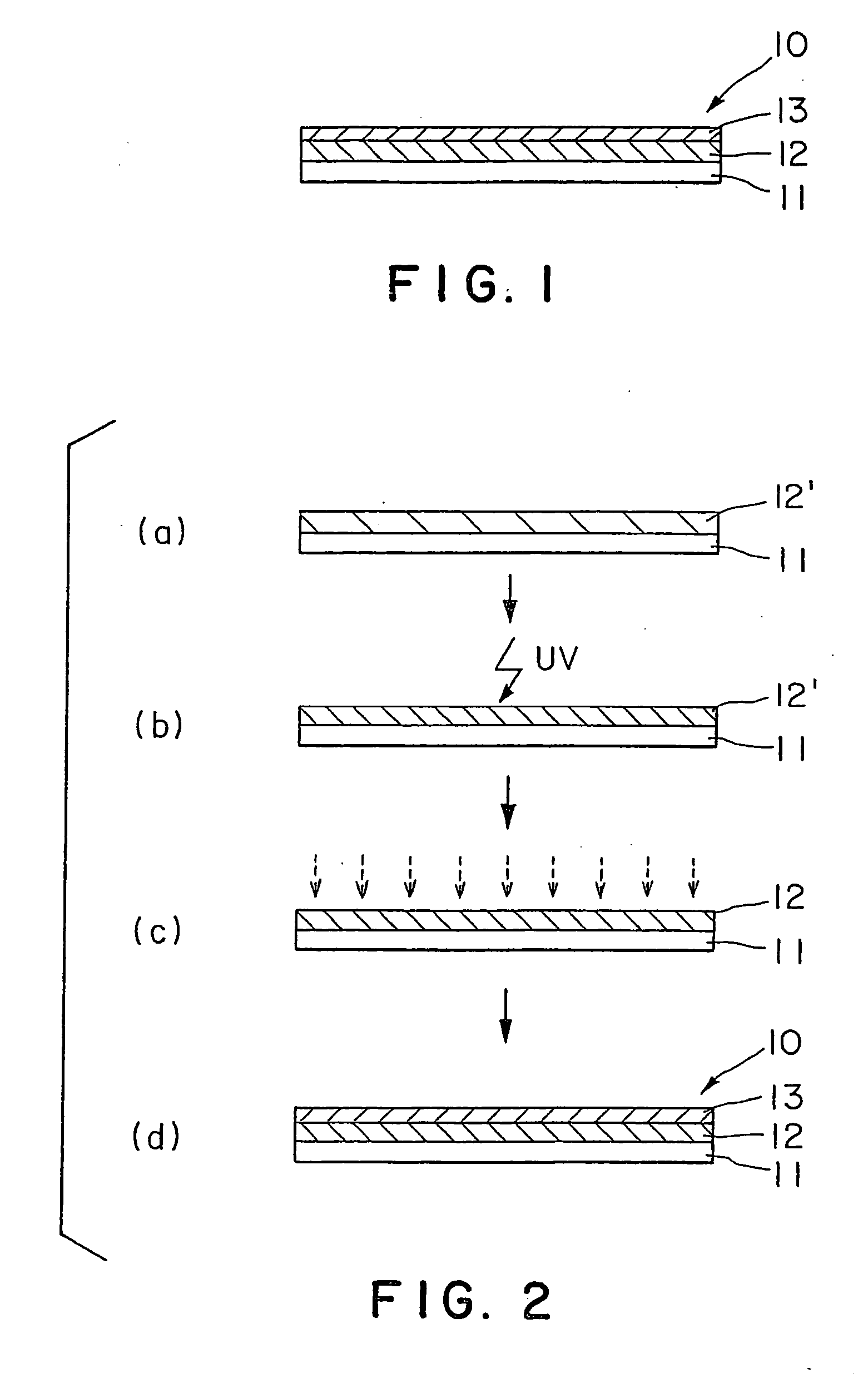
[0058] A polyimide film (LX1400 (manufactured by Hitachi Chemical Co., Ltd., Japan)) with a thickness of 0.02 μm was formed on a glass substrate. After baked at 250° C, the polyimide film was then subjected to rubbing treatment for alignment.

[0059] The rubbed polyimide film on the glass substrate was spin-coated with a solution containing a cholesteric liquid crystal having a composition as described below.

[0060] Nematic liquid crystal (above formula (8)): 95.45% by weight

[0061] Chiral agent (above formula (14)): 4.55% by weight

[0062] Polymerization initiator (Irg907): 5% by weight Surface active agent (below formula (15)): 0.05% by weight

[0063] Toluene: 175% by weight

[0064] As described above, the cholesteric liquid crystal solution contains a cholesteric liquid crystal (chiral nematic liquid crystal) which is a mixture of a nematic liquid crystal and a chiral agent.

[0065] The coating film applied to the polyimide film on the glass substrate was subjected to a treatment for...

example 3

[0070] An optical element was produced in the same manner as that of Example 1, other than that JSS-341 (manufactured by JSR Corporation) was used as a material for forming a protective layer, with its thickness being 1.5 μm, and that the protective layer was not subjected to exposure process when forming the protective layer. The modulus of elasticity of thus obtained optical element according to Example 3 was determined by pushing, from the protective layer side, an indenter into the cholesteric liquid crystal layer with a test force of 2 mN in accordance with the universal hardness test method. As a result, the modulus of elasticity was 0.65, and the plastic deformation was 0.46 μm. A protective layer was formed directly on a glass substrate in the same manner as that of Example 1, and its modulus of elasticity was determined by pushing an indenter into the protective layer with a test force of 2 mN in accordance with the universal hardness test method. As a result, the modulus o...

example 4

[0071] An optical element was produced in the same manner as that of Example 1, other than that an ITO layer (1500 Åthickness) as a transparent electrode was formed on a surface of a protective layer by spattering, and then a polyimide film (LX1400 (manufactured by Hitachi Chemical Co., Ltd., Japan); 0.07 Hm thickness) as an alignment film was formed on the ITO layer. The polyimide film on the ITO layer was formed in the same manner as the alignment film on a glass substrate in Example 1. The modulus of elasticity of thus obtained optical element according to Example 4 was determined by pushing, from the protective layer side, an indenter into the cholesteric liquid crystal layer with a test force of 2 mN in accordance with the universal hardness test method. As a result, the modulus of elasticity was 0.66, and the plastic deformation was 0.46 μm. A protective layer was formed directly on a glass substrate in the same manner as that of Example 1, and its modulus of elasticity was de...


PUM

PropertyMeasurementUnit
indentation forceaaaaaaaaaa
thicknessaaaaaaaaaa
thicknessaaaaaaaaaa

Abstract

An optical element including: an alignment substrate; a liquid crystal layer formed on the alignment substrate, made by forming and curing a film of a liquid crystalline material; and a protective layer having high hardness, formed on the liquid crystal layer. The protective layer is for protecting the liquid crystal layer from being deformed by externally exerted forces. Preferably, the protective layer has a modulus of elasticity (=(elastic deformation) / (total deformation)) of 0.6 or more and a plastic deformation of 0.5 μm or less as determined by pushing an indenter into the protective layer with a test force of 2 mN in accordance with the universal hardness test method. The optical element has the advantages that the film thickness distribution of the liquid crystal layer remains uniform even when forces are externally exerted to the optical element in the process of production of the optical element or in the course of incorporation of the optical element in a liquid crystal display, and that the optical element can maintain its high displaying quality even when incorporated in a liquid crystal display.

Description

[0001] This is a Continuation of U.S. patent application Ser. No. 10 / 629,908 filed Jul. 30, 2003. The entire disclosure of the prior application is hereby incorporated by reference in its entirety.BACKGROUND OF THE INVENTION [0002] 1. Field of the Invention [0003] The present invention relates to an optical element, such as a polarized-light-separating element, a color filter, and a retardation film, for use in a liquid crystal display and the like. More particularly, the present invention relates to an optical element including a liquid crystal layer made from a liquid crystalline material such as a cholesteric liquid crystal and a nematic liquid crystal. The term “liquid crystal layer” as used herein refers to a layer having the nature of liquid crystal in an optical sense, and encompasses a layer in the solidified state that a liquid crystal phase is solidified with its molecular orientation maintained as it is. [0004] 2. Description of Related Art [0005] In general, a convention...

Claims


Application Information

Patent Timeline
Patent Type & Authority Applications(United States)
IPC IPC(8): G02F1/1333G02B1/10G02B5/30
CPCG02B1/105G02B5/3016G02B5/3033G02B5/3083G02F2001/133543G02F1/133516G02F1/133636G02F1/13718G02F2001/133521G02F1/133514G02B1/14G02F1/133521G02F1/133543
Inventor TAZAKI, KEIKOISHIZAKI, KOJI
Owner DAI NIPPON PRINTING CO LTD
Why Eureka
Try Eureka