Electrophotographic photoconductor
- Summary
- Abstract
- Description
- Claims
- Application Information
AI Technical Summary
Benefits of technology
Problems solved by technology
Method used
Image
Examples
first embodiment
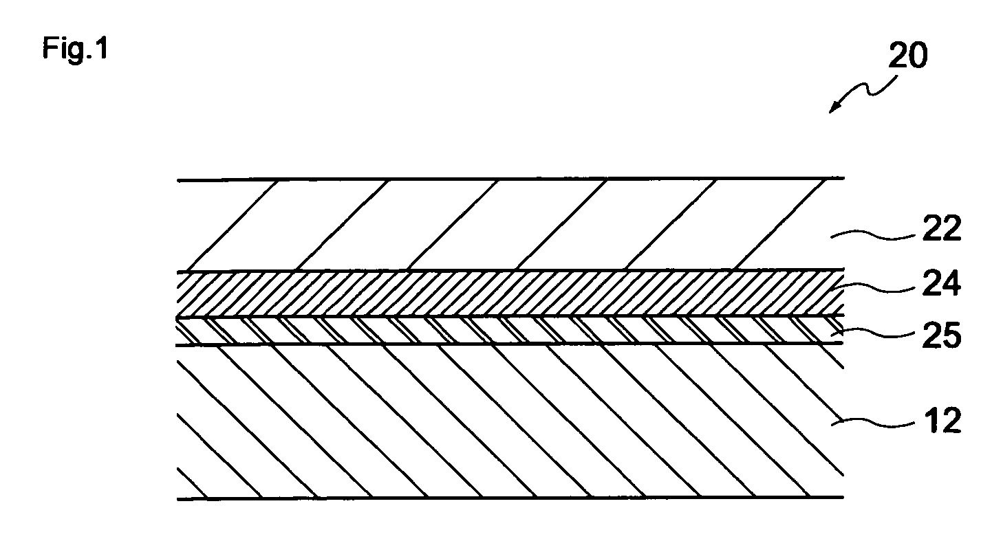
[0051] As exemplified in FIG. 1, a first embodiment of the present invention is an electrophotographic photoconductor having a conductive substrate on which a photosensitive layer containing at least a charge generating agent, a hole transfer agent and a binding resin is provided. The electrophotographic photoconductor is characterized in that the binding resin is comprised of a plurality of polycarbonate resins and the photosensitive layer contains a biphenyl derivative as a plasticizer component.
[0052] Hereinafter, the multilayer-type electrophotographic photoconductor in accordance with the first embodiment of the present invention will be concretely described.
1. Supporting Substrate
[0053] As a supporting substrate 12 as exemplified in FIG. 1, any of various materials having conductivities can be used. For instance, the materials include metals such as iron, aluminum, cupper, tin, platinum, vanadium, molybdenum, chrome, cadmium, titanium, nickel, palladium, indium, stainless ...
example 2
(2)-3 Concrete Example 2
[0153] Furthermore, the concrete examples of the hole transfer agent include compounds represented by the following formulae (21) to (24) (HTM-1 to 4).
(2)-4 Amount Added
[0154] Furthermore, it is characterized in that the amount of the hole transfer resin added is in the range of 1 to 100 parts by weight with respect to 100 parts by weight of the binding resin.
[0155] This is because, when the amount of the hole transfer agent added is less than 1 part by weight, the sensitivity of the photoconductor layer cannot be retained after carrying out a given continuous printing.
[0156] In contrast, when the amount of the hole transfer agent added exceeds 100 parts by weight, it may become difficult to be uniformly mixed and dispersed or may tend to crystallize.
[0157] Therefore, the addition amount of the hole transfer agent added may be preferably in the range of 5 to 80 parts by weight, more preferably in the range of 10 to 50 parts by weight with respect to 10...
second embodiment
[0222] As illustrated in FIG. 5, a second embodiment of the present invention is an electrophotographic photoconductor 30 having a monolayer-type photosensitive layer 26 containing at least a charge generating agent, a hole transfer agent and a binding resin and formed on a conductive substrate 12. The electrophotographic photoconductor 30 is characterized in that a plurality of polycarbonate resins is used as the binding resin and the photosensitive layer 26 contains a biphenyl derivative as a plasticizer component.
[0223] Hereinafter, the electrophotographic photoconductor as a monolayer-type photoconductor in accordance with the second embodiment of the present invention will be concretely described.
1. Basic Configuration
[0224] Regarding to the type and so on with respect to the basic configuration of the monolayer-type photoconductor, but not specifically limited to, the thickness of a photoconductor layer may be generally in the range of 5 to 100 μm, preferably in the range ...
PUM
| Property | Measurement | Unit |
|---|---|---|
| Temperature | aaaaa | aaaaa |
| Fraction | aaaaa | aaaaa |
| Time | aaaaa | aaaaa |
Abstract
Description
Claims
Application Information


