Optical element and its manufacturing method

a manufacturing method and technology of optical elements, applied in the field of optical elements, can solve the problems of reducing the production yield, shrinking and peeling of the insulation material covering the side surfaces of the first and second columnar sections, and reducing the yield, so as to achieve high efficiency, reduce leakage current, and reduce yield

Inactive Publication Date: 2007-03-08
SEIKO EPSON CORP
View PDF6 Cites 0 Cited by
  • Summary
  • Abstract
  • Description
  • Claims
  • Application Information

AI Technical Summary

Benefits of technology

[0009] In accordance with an advantage of some aspects of the present invention, it is possible to provide highly efficient optical elements without electrode disconn

Problems solved by technology

When the process for manufacturing optical elements includes the step of heating the optical element after the insulation layer has been formed, there is a possibility that the insulation material covering the side surfaces of the first and second columnar sections may shrink and peel off from the side surfaces of the columnar sections.
Also, when the process includ

Method used


Image

  • Optical element and its manufacturing method
  • Optical element and its manufacturing method
  • Optical element and its manufacturing method

Examples


Embodiment Construction

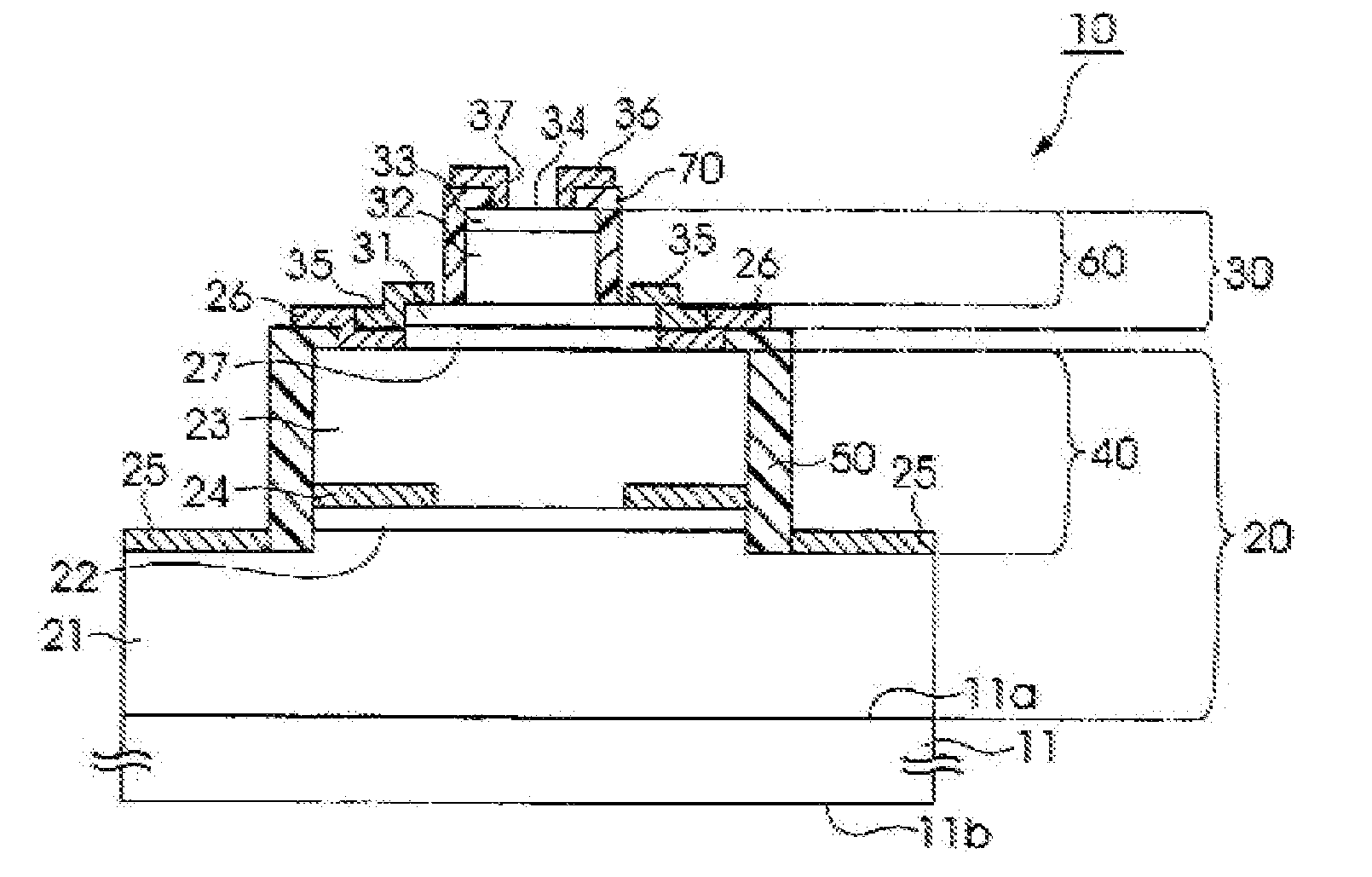
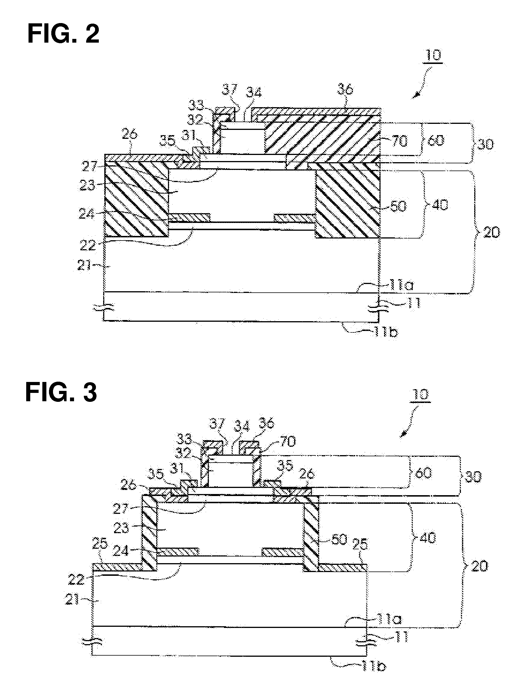
[0051] An optical element and its manufacturing method in accordance with an embodiment of the invention are described in detail with reference to the accompanying drawings. It is noted that the embodiment to be described below indicates a part of modes of the invention, does not limit the invention, and can be appropriately modified within the scope of the invention. Also, in the drawings referred to below for describing the invention, the scale may be changed for each of the layers and each of the members such that the layers and the members can have appropriate sizes that can be recognized on the drawings.

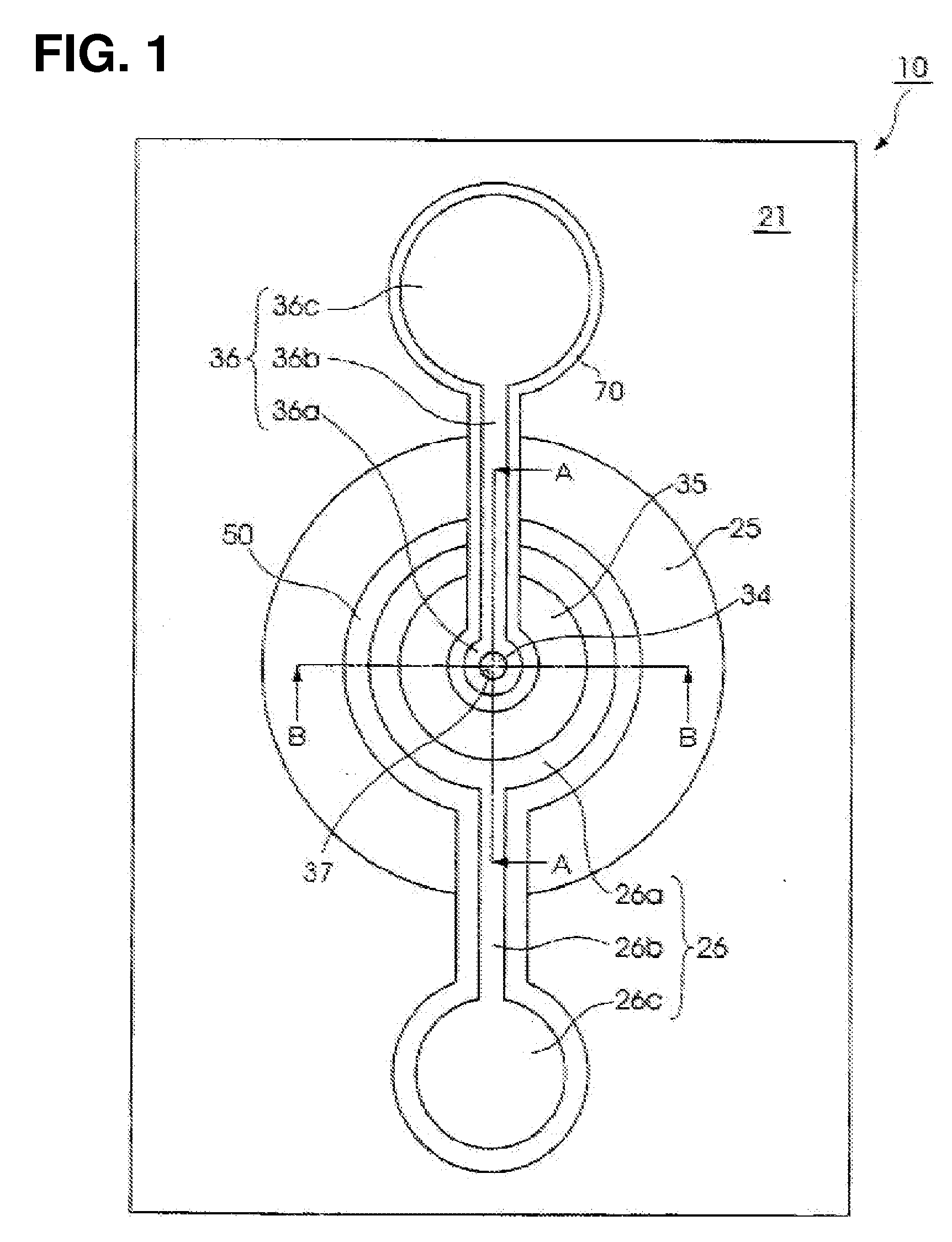
[0052] Structure of Optical Element

[0053] First, the structure of an optical element in accordance with an embodiment of the invention is described with reference to FIGS. 1 through 3. FIG. 1 schematically shows a plan view of the optical element in accordance with the embodiment of the invention, and FIG. 2 and FIG. 3 schematically show cross-sectional views of the optical el...


PUM


Abstract

An optical element includes a substrate, a surface-emitting type semiconductor laser that emits laser light in a direction vertical to a surface of the substrate, and a light-receiving element formed above or below the surface-emitting type semiconductor laser provided above the substrate. The optical element includes a first insulation layer that covers a side surface and a part of an upper surface of a first columnar section that includes at least a part of the surface-emitting type semiconductor laser, and a second insulation layer that covers a side surface and a part of an upper surface of a second columnar section that includes at least a part of the light-receiving element.

Description

[0001] The entire disclosure of Japanese Patent Application No.2005-258893, filed Sep. 7, 2006 and No.2006-165760, filed Jun. 15, 2006 are expressly incorporated by reference herein. BACKGROUND [0002] 1. Technical Field [0003] The present invention relates to optical elements that emit laser light and methods for manufacturing the same. [0004] 2. Related Art [0005] A surface-emitting type semiconductor laser is a type of optical elements that emit laser light. The surface-emitting type semiconductor laser is provided with a resonator formed in a direction vertical to a surface of the substrate, and emits laser light from the substrate surface. Compared to conventional edge-emitting type semiconductor lasers that use horizontal cleavage surfaces of a substrate as a resonator, the surface-emitting type semiconductor laser has various characteristics. For example, surface-emitting type semiconductor lasers are suitable for mass-production, capable of direct modulation, and capable of o...

Claims


Application Information

Patent Timeline
IPC IPC(8): H01L21/16
CPCH01S5/0264H01S5/0425H01S2301/18H01S2301/176H01S5/18313H01S5/04257H01S5/04256
Inventor KANEKO, TSUYOSHIIMAI, YASUTAKA
Owner SEIKO EPSON CORP
Why Eureka
Try Eureka