Ultra-high resolution pixel electrode arrangement structure signal processing method
- Summary
- Abstract
- Description
- Claims
- Application Information
AI Technical Summary
Benefits of technology
Problems solved by technology
Method used
Image

Examples
example 1
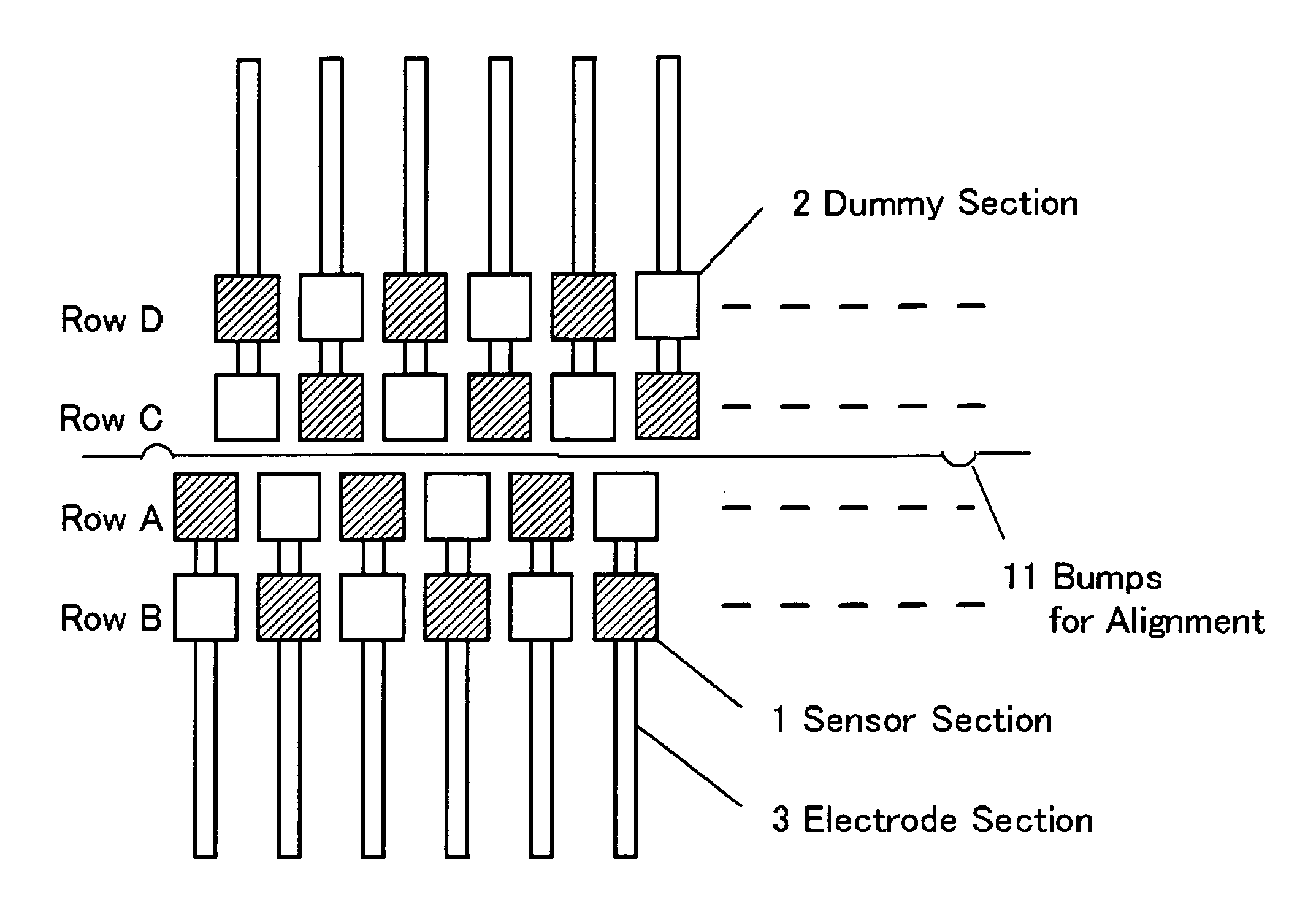
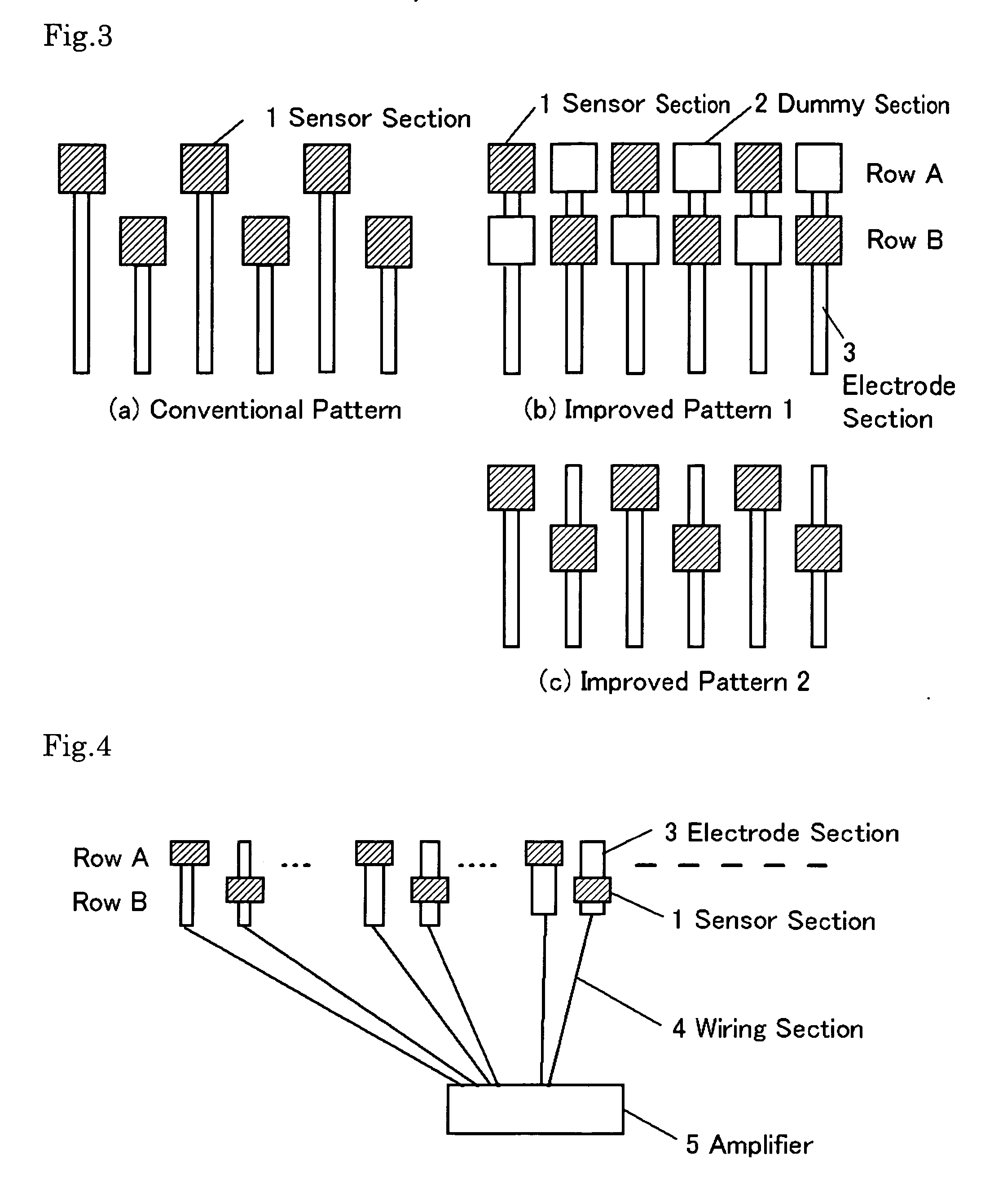
[0028]FIG. 3 shows the patterns of the electrode sections 3 on a board on which a sensor is mounted. FIG. 3-a is a conventional pattern where capacitance is not uniform since the lengths of the electrode sections 3 are different. In the case of the improved pattern in FIG. 3-b according to the present invention, the electrode sections 3 are patterned in the same way whether it is an odd number or even number even if a staggered arrangement is used, in order to make the capacitance uniform. In other words, capacitance differs because of the difference in the lengths of the wires, which makes voltage, to be generated from the same charges, different, and causes output variations, so in order to prevent this the same electrode structure is used, where a portion in which an element is mounted is laid out as the sensor section 1, and a portion in which an element is not mounted becomes a dummy section 2, where the electrode section 3 remains as is. The mounted elements result in a stagge...
example 2
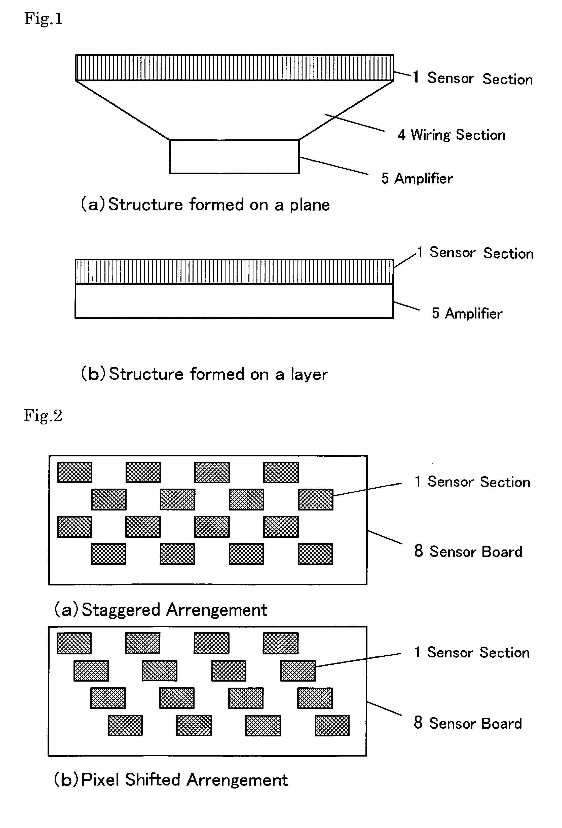
[0033]FIG. 5 shows an example of the boards, on which the elements are arranged in staggered positions, disposed so as to face each other in order to double the number of pixels to further increase resolution.
[0034]FIG. 5 is an example when two rows of staggered elements are facing the other two rows of elements with a shifted ¼ pitch from each other. By combining the respective two rows of staggered elements like this, four elements spatially constitute one pitch. If this configuration is used, signals are read alternately between the two boards facing each other, so an element can be read after the leak signal from its adjacent element attenuates, so the mutual influence of the signals of an adjacent element can be prevented.
[0035] If one block of a staggered arrangement is disposed with another one facing each other with a shifted ¼ pitch, then a pixel shifted arrangement can be easily implemented.
[0036] If the amplifiers for the element rows facing each other are installed is...
example 3
[0043] In the above description, the wiring section from the electrode section of the sensor to the amplification section is one used for a one-dimensional sensor, that is a linear type line sensor. However recent demands for a two-dimensional sensor is high. So [Example 3] proposes a connection to the amplification section in a two-dimensional sensor.
[0044] In FIG. 6, the electrode sections, which are led out from the two-dimensional sensor 9, are arranged two-dimensionally on the bottom face of the sensor. Each row of the two-dimensional terminals is connected to the amplification section 5 via a flexible wire 10. If the two-dimensional terminal is S (m, n), then S (1, j) (j is an integer in the 1- - - n range) is connected to one flexible wire 10, and m number of flexible wires 10 are used. In FIG. 6, S (1, 1), S (1, 2), . . . S(2, 1), S (2, 2) . . . are connected sequentially from the front of the amplification section 5, but may be in the sequence of S (1, 1), S (2, 1), S (3, ...
PUM
 Abstract
Description
Claims
Application Information
PatSnap Eureka turns technology decisions into work you can execute. Powered by our Innovation Knowledge Graph, it runs expert workflows across engineering, life sciences, materials and intellectual property. Get your review-ready output in minutes.


