
Integrated circuit device

Inactive Publication Date: 2003-10-02
FUJIFILM BUSINESS INNOVATION CORP
View PDF13 Cites 41 Cited by
  • Summary
  • Abstract
  • Description
  • Claims
  • Application Information

AI Technical Summary

Benefits of technology

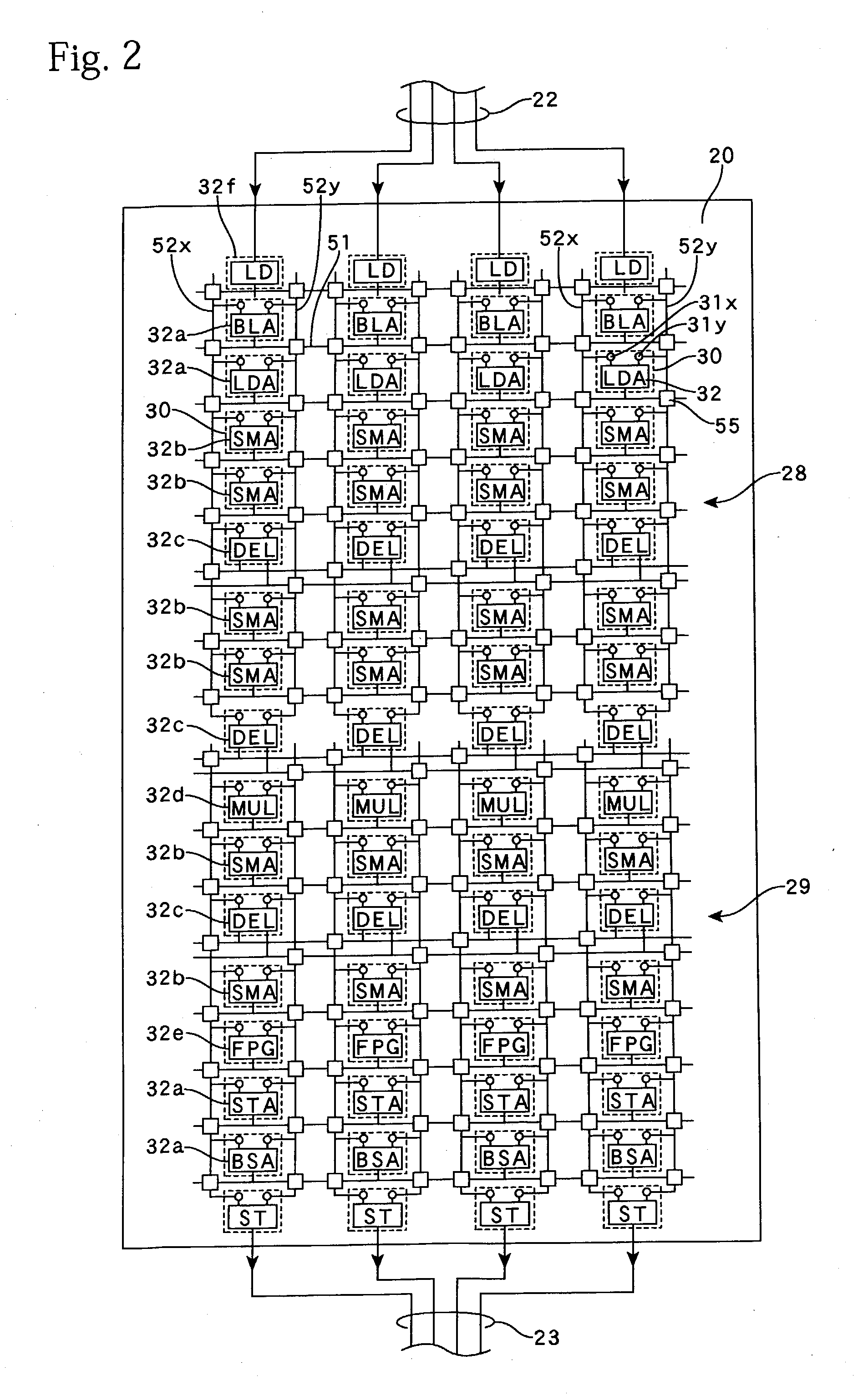
[0009] In the present specification, the expression "operation units" refers to small-scale units that (1) process data in byte or word unit, (2) are equipped with data paths which are suited to special-purpose or specific processing, and (3) can execute a special-purpose or specific arithmetic operation, a special-purpose or specific logic operation, or a combination of such. These operation units are also referred to as elements, logic elements, logic units or circuit units. The area required to produce a plurality of types of operation units that include different or unique data paths that are suited to special-purpose processing on a semiconductor substrate is likely to differ for each type of operation units. However, for operation units of the same type, the occupied area is the same. Accordingly, by having operation units of the same type form an arrangement in a first direction or in a second direction, fluctuations due to differences in the sizes of operation units is eliminated. If the first direction is a row direction (the horizontal direction, lateral or width direction), the second direction is the column direction (the vertical direction, longitudinal or height direction). As one example, if operation units of the same type form an arrangement in the first direction, the plurality of operation units can be arranged so as to form a straight band with an even width. Accordingly, a plurality of operation units, for which the data path differs according to the type and whose sizes are likely to be different, can be arranged in a straight line in the first direction without generating redundant space in the second direction. Since the operation units are aligned in the first direction in a straight line without size fluctuations, it is possible to lay out at least the wire sets in the first direction in a straight line. This makes it possible to increase the area efficiency and the integration of an integrated circuit device in which operation units including different data paths are arranged in a matrix, so that an economical integrated circuit device that has a high processing speed and favorable AC characteristics can be provided.
[0028] For the integrated circuit device that can be controlled by a program, an execution program of the integrated circuit device can be generated by (i) intermediate description for the process to be executed in a programming language that includes instructions which are supported by the operation units and (ii) including instructions that indicate the execution configuration of the plurality of types of operation units that can execute this intermediate description. It is preferable for the intermediate language to be an assembler-like language with high linearity so that data flowgrams are easy to produce.

Problems solved by technology

Accordingly, the area efficiency is low relative to the functions that can be realized, and the computation speed is also not particularly high.
When the functions to be realized by an FPGA are changed, the functions of an extremely large number of logic blocks have to be changed, so that it is hard to make dynamic changes.
Even if it is possible to reduce the time required to change the functions by providing special hardware for directly controlling each logic block separately, it is still difficult to dynamically control such special hardware during the execution of an application and this solution is not economic.
However, this lowers the area efficiency, which results in an integrated circuit being extremely large, and also causes a deterioration of the AC characteristics.
This makes it impossible to fully achieve the basic merits of an integrated circuit device composed of operation units with data paths that are suited to special-purpose processing.
When the number of one type of operation unit, for example, a first type of operation unit, is much higher than the number of a second type of operation unit, if the first type of operation units are positioned simply in accordance with the length of the arrangements of the second type of operation units, the overall shape of the data processing block ends up being too long and thin, which may reduce the area efficiency.
When the sizes of the various types of operation units in the first direction are different, the most efficient arrangement in the second direction cannot be achieved.
When the number of operation units included in a matrix increases, if these operation units are connected in a flexible manner, the required amount of wiring corresponds to the operation units, so that an extremely large amount of wiring becomes necessary.
Although the data processing block of this integrated circuit device has an overall general applicability whereby different processing can be performed, each of the operation units is a special-purpose circuit unit with a data path that is suited in advance to special-purpose or specific processing, making the applicability of each operation unit low.

Method used


Image

  • Integrated circuit device
  • Integrated circuit device
  • Integrated circuit device

Examples


Embodiment Construction

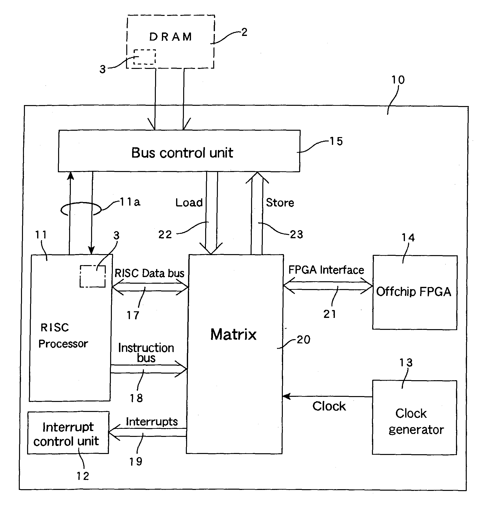
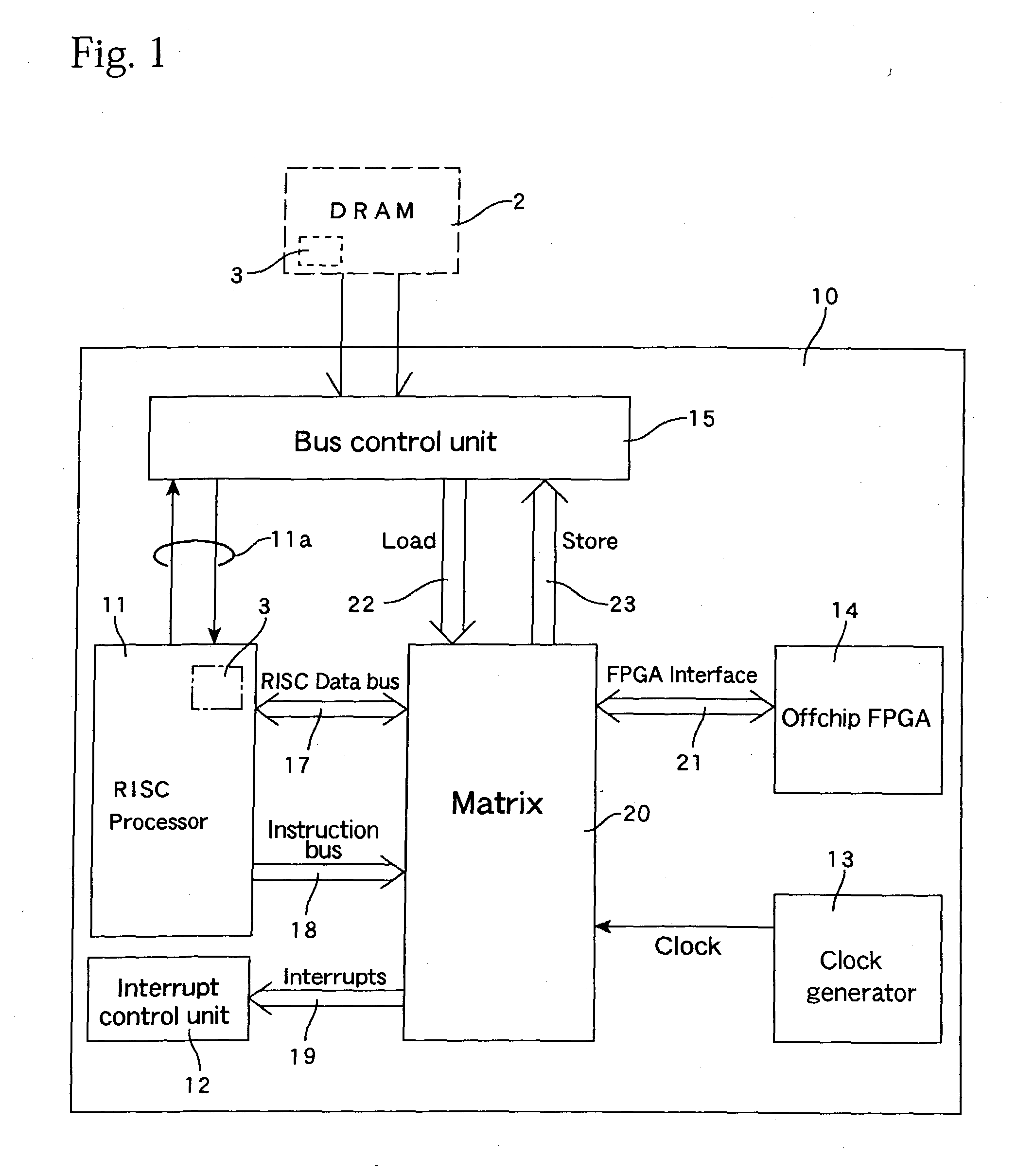
[0051] The following describes the present invention with reference to the attached drawings. FIG. 1 shows an example where a system LSI 10 is configured as an integrated circuit device according to the present invention. This system LSI 10 includes a general-purpose processor 11, such as a RISC processor for performing general-purpose processing, includes error handling, based on instructions in an execution program 3, and a data processing block (hereafter referred to as the "matrix unit" or "matrix") 20 where a data flow or a pseudo data flow that is suited to special-purpose data processing is formed by a plurality of operation units that are arranged in a matrix. The general-purpose processor (hereafter also referred to as the "RISC") 11 also controls the configuration of the matrix 20 based on the execution program 3, so that the configuration of the matrix 20 can be dynamically changed. The system LSI 10 also includes an interrupt control unit 12 for controlling the handling ...


PUM


Abstract

An integrated circuit device with a data processing block is provided, the data processing block including a plurality of operation units that are arranged in a matrix, a plurality of first wire sets that extend in a first direction in the matrix and transfer input data of each operation unit, a plurality of second wire sets that extend in a second direction in the matrix and transfer output data of each operation unit, and a plurality of switching units that are arranged at each intersection between the first and second wire sets and can select and connect any wire in the first wire sets and any wire in the second wire sets. The plurality of operation units include a plurality of types of operation units with different data paths that are suited to special-purpose, processing, with an arrangement of operation units of the same type in the first direction or the second direction being formed in at least part of the data processing block. The functioning of the integrated circuit device can be dynamically changed by changing the configuration of the operation units and the integrated circuit device is composed of operation units with different data paths that are suited to special-purpose processing so that the integrated circuit device is both compact and economical.

Description

[0001] The present invention relates to an integrated circuit device in which a plurality of operation units are arranged in a matrix.RELATED ART[0002] FPGA (Field Programmable Gate Arrays) are conventionally known as integrated circuit devices in which logic gates are laid out in arrays and the interconnects between the logic gates can be freely changed. The construction of an FPGA can be roughly classified into a plurality of logic blocks and wiring that connects these logic blocks. A logic block is a circuit unit that includes a lookup table and a flip-flop, and, by changing the set values in the lookup table, functions as a logic gate for achieving a logic function, such as an AND or an OR, in bit units. A plurality of logic blocks are arranged in an array or in a matrix and are connected by row wires and column wires. Row wires and column wires are connected by switch matrices or the like at the intersections between the wires so that the wiring can be reconfigured. By reconfig...

Claims


Application Information

Patent Timeline
IPC IPC(8): G06F15/78G06F17/50
CPCG06F17/5045G06F15/7867G06F30/30H03K19/173
Inventor IKEDA, KENJISHIMURA, HIROSHISATO, TOMOYOSHI
Owner FUJIFILM BUSINESS INNOVATION CORP
Learn More