Semiconductor memory module, memory system, circuit, semiconductor device, and DIMM

a memory module and semiconductor technology, applied in the field of bus connection technique, can solve the problems of short timing margin, inability to allow time difference due to a wiring length difference, and low wiring efficiency

Inactive Publication Date: 2006-08-22
LONGITUDE SEMICON S A R L
View PDF19 Cites 41 Cited by
  • Summary
  • Abstract
  • Description
  • Claims
  • Application Information

AI Technical Summary

Benefits of technology

[0015]Hence, in view of these problems, a first object of the present invention is to provide a system, in which the timing of data signals, C / A signals, and clock signals is matched so as to permit the wiring length difference, by means of a method of implementing them at lower costs and without increasing the wiring density and the number of substrate layers.
[0016]Also, a second object of the present invention is to provide a system for eliminating the wiring length difference between the C / A signals and the clock signals and having consistency in the timing of both signals.
[0021]By using the first means to solve the above first problem, the DRAM is such that the clock timing adjustment circuit allows the DRAMs to adjust the clock signal timing by the delay time due to wiring-lenght difference between the clock signals and the C / A signals, thereby latching the C / A signals by the clock signals having the adjusted timing.
[0022]Also, by using the second means to solve the first problem, the DRAM is such that the C / A signal timing adjustment circuit allows the DRAMs to adjust the C / A signal timing by a delay time due to the wiring-length difference between the clock signals and the C / A signals, thereby latching the C / A signals having the adjusted timing by the clock signals.
[0023]By using the first means to solve the second problem, the time difference between the C / A signals and the second clock signals is almost eliminated, and the DRAMs can latch the C / A signals by the second clock signals.

Problems solved by technology

However, wiring efficiency thereof is not so high.
However, as the operating frequency of the C / A signal 51 is increased, the timing margin becomes short and the time difference due to a wiring length difference cannot be finally permitted.
This is fundamentally caused by the problem that the clock signals 50A and the C / A signals 51A use different wiring schemes.

Method used


Image

  • Semiconductor memory module, memory system, circuit, semiconductor device, and DIMM
  • Semiconductor memory module, memory system, circuit, semiconductor device, and DIMM
  • Semiconductor memory module, memory system, circuit, semiconductor device, and DIMM

Examples


first embodiment

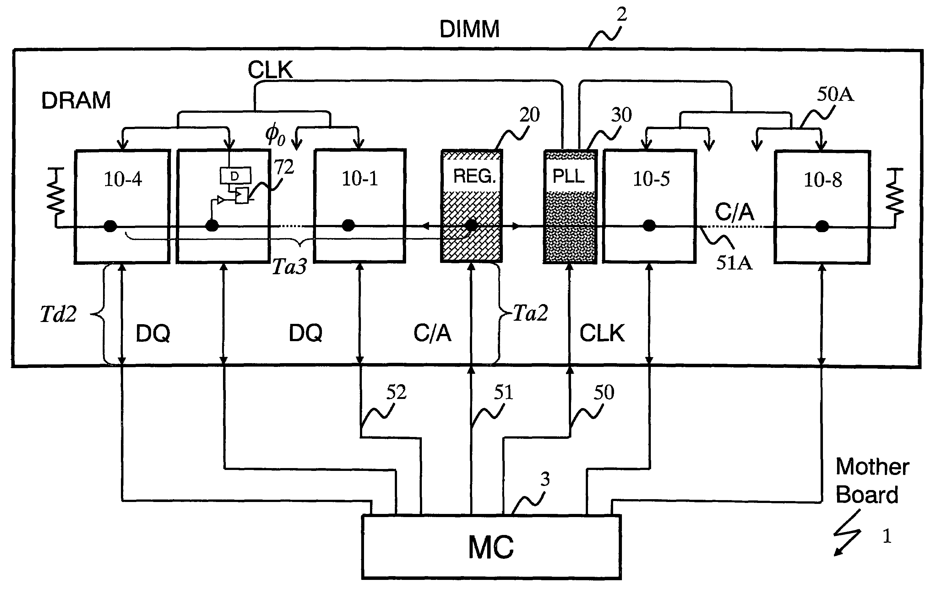
[0047]A first embodiment will be described with reference to FIG. 1.

[0048]The reference numerals “10-1” to “10-8” denote DRAMs mounted on a DIMM 2. In addition to the DRAMs 10-1 to 10-8, the DIMM 2 incorporates a C / A register 20 (hereafter abbreviated as “register”) for command / address signals and a clock signal stabilizing circuit (hereafter abbreviated as “PLL”) 30.

[0049]A memory controller (hereafter abbreviated as “MC”) 3 executes control of reading and writing of signals to the DRAMs 10-1 to 10-8, and is mounted on a print circuit board (hereafter abbreviated as “motherboard”) 1. To the respective DRAMs 10-1 to 10-8 from the MC 3, terminals on which the DIMM 2 is mounted are connected through wirings on the motherboard 1.

[0050]A C / A signal 51 is transmitted from the MC 3 to a register 20 mounted on the DIMM 2, and connected from the register 20 to each of the DRAMs 10-1 to 10-8 on the DIMM 2. The reference numeral “51A” denotes a signal within the DIMM 2. In FIG. 1, the registe...

second embodiment

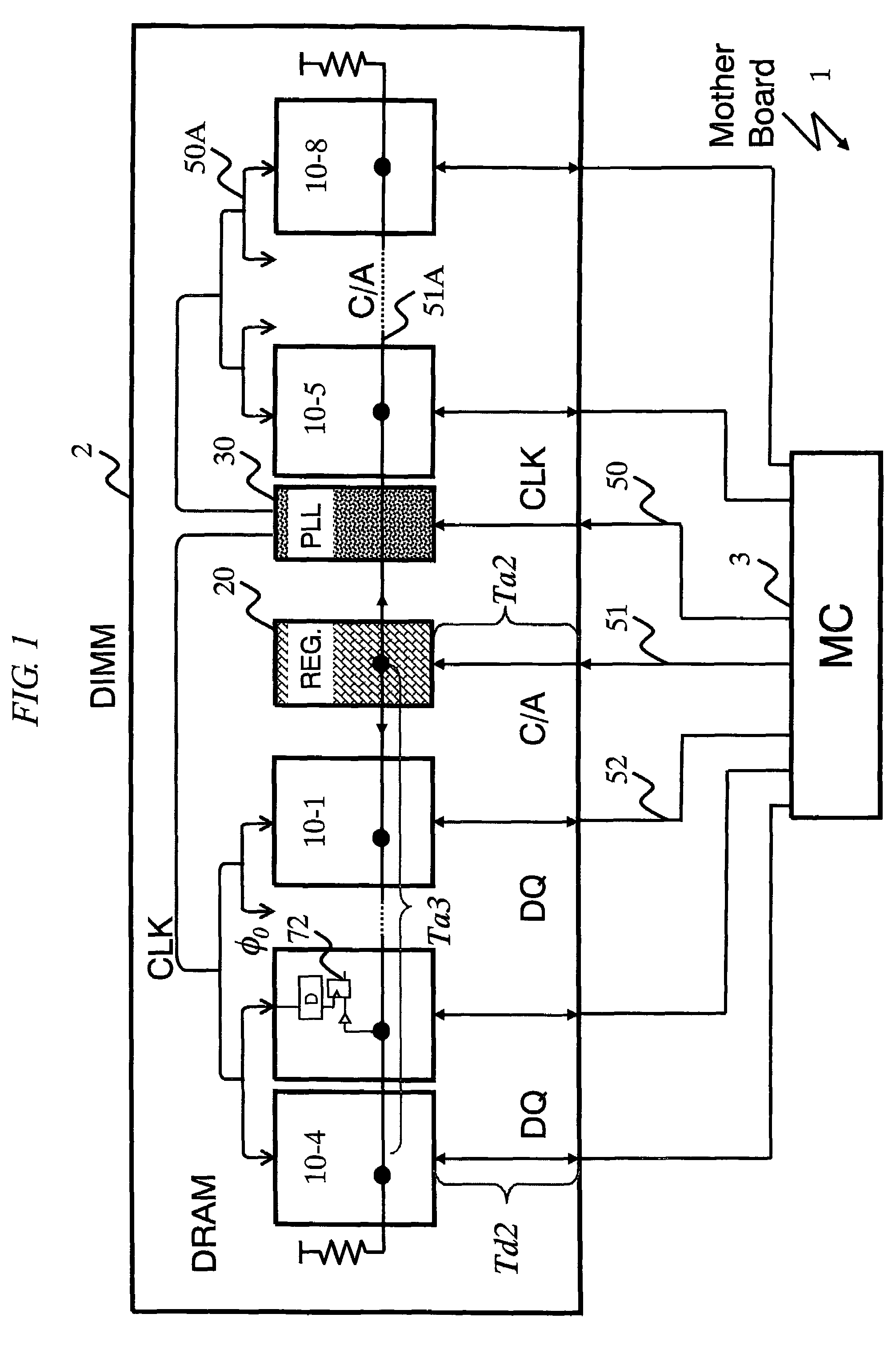
[0076]With reference to FIG. 6 a second embodiment will be described.

[0077]The present embodiment is characterized in that the same line is used for a clock for receiving the C / A signals and for a clock distributed to each DRAM.

[0078]On the DIMM 2, the DRAMs 10-1 to 10-8, the register 20, and the PLL 30 are mounted. The register 20 and the PLL 30 are located at an end of the DIMM 2. Then, C / A signals 51B in the DIMM 2 are wired into a daisy-chain shape. Also for clock signals 50B, a folded wiring from the PLL 30 is used, and clock-input terminals of the DRAMs 10-1 to 10-8 are respectively connected to the wiring before folding and that after folding. In addition, as a far end of the wiring of the clock signals 50B is a matching end, there is no reflection at this part.

[0079]In order to adopt this configuration, two clock signals having a different phase in accordance with a wiring-length difference are inputted to the DRAMs 10-1 to 10-8. If terminals are denoted by the reference num...

third embodiment

[0090]A third embodiment will be described with reference to FIG. 10.

[0091]The present invention is an example in which the clock signals 50B in the second embodiment are constituted by a directional coupler. FIG. 10 shows only the clock signals and the C / A signals, and other signals are the same as those in the second embodiment. In this embodiment, the clock signals are denoted by the reference numeral “50C”. In addition, although four DRAMs is used to simply describe this embodiment, the same effects can be achieved irrespective of whether the number of the DRAMs is smaller or greater. One wiring for the clock signals 50 is drawn from the PLL in (register+PLL) 21, and a far end of the above wiring is an open end. Thus, the clock signals 50C outputted from the PLL are totally reflected at the far end. The totally reflected pulses are absorbed by the termination resistor provided in the PLL and are not reflected again.

[0092]By using, as a primary coupling wiring, the wiring of the ...


PUM


Abstract

There is the problem that since C / A signals in a DIMM are distributed to respective DRAMs through a register in the DIMM and DQ signals are wired directly from terminals in the DIMM, their timing is difficult to synchronize. The register for speeding up the C / A signals of the DIMM that operates with high speed is provided, and a wiring from the register is set to a daisy-chain wiring. Then, by a timing adjustment circuit provided in the DRAM, a wiring delay time difference between the C / A signals and the clock signals, which are different depending on positions of the DRAMs, is such that the sum of a delay time from the register to each DRAM and a delay amount due to the timing adjustment circuit is made equal to a delay time of the farthest DRAM.

Description

CROSS-REFERENCE TO RELATED APPLICATION[0001]The present application claims priority from Japanese patent application No. JP 2003-428621 filed on Dec. 25, 2003 and No. JP 2004-364743 filed on Dec. 16, 2004, the contents of which are hereby incorporated by reference into this application.BACKGROUND OF THE INVENTION[0002]The invention relates to a bus connecting technique for connecting a processor and functional circuits, which is used in an information processing apparatus, and to components thereof.[0003]As a data rate is enhanced, a time for propagating a wiring between devices becomes increasingly equal to a data cycle. In particular, in a memory technique called a DDR (Double Data Rate)-SDRAM, an operating frequency of a command signal / address signal (hereinafter abbreviated as “C / A signal”) is half of that of a data signal (hereinafter abbreviated as “DQ signal”). For example, in currently available products, data has a transfer rate of 400 Mbps while address has half of the tra...

Claims


Application Information

Patent Timeline
Patent Type & Authority Patents(United States)
IPC IPC(8): G11C99/00G06F12/00G06F1/10G06F13/16G11C7/10G11C7/22G11C8/00G11C11/4076G11C11/4093G11C29/02
CPCG11C7/1051G11C7/106G11C7/1066G11C7/1078G11C7/1087G11C7/1093G11C29/50012G11C7/222G11C11/4076G11C11/4093G11C29/02G11C29/028G11C7/22G11C11/401
Inventor OSAKA, HIDEKINISHIO, YOJIFUNABA, SEIJI
Owner LONGITUDE SEMICON S A R L
Why Eureka
Try Eureka