Strained semiconductor device and method of making the same

a technology of semiconductor devices and strainers, applied in the direction of semiconductor devices, electrical devices, transistors, etc., can solve the problem that the effect of mechanical stress on the performance of transistors is not guaranteed for all transistors, and achieve the effect of improving transistor performance and carrier mobilities

Inactive Publication Date: 2007-03-15
INFINEON TECH AG
View PDF37 Cites 60 Cited by
  • Summary
  • Abstract
  • Description
  • Claims
  • Application Information

AI Technical Summary

Benefits of technology

[0007] In the prior art, as described above, trenches are etched next to transistor gates. These trenches are filled with epitaxial SiGe or other material that has a different lattice constant than silicon. Due to the different lattice constants or thermal expansion coefficients, mechanical stress is produced and issued onto the transistor channel, resulting in improved carrier mobilities and thus improved transistor performance.
[0009] In one aspect, the present invention provides a self-aligned etching and filling of grooves or recesses in silicon (or another semiconductor) in the neighborhood of a gate. The preferred method assures a uniform length of the trenches resulting in a uniform filling with equivalent amounts of material. One advantage is that the trenches can be designed uniformly over the wafer surface. This allows for good stress optimization.

Problems solved by technology

Therefore, an equal impact of the mechanical stress on the transistor performance is not guaranteed for all transistors.

Method used


Image

  • Strained semiconductor device and method of making the same
  • Strained semiconductor device and method of making the same
  • Strained semiconductor device and method of making the same

Examples


Embodiment Construction

[0020] The making and using of the presently preferred embodiments are discussed in detail below. It should be appreciated, however, that the present invention provides many applicable inventive concepts that can be embodied in a wide variety of specific contexts. The specific embodiments discussed are merely illustrative of specific ways to make and use the invention, and do not limit the scope of the invention.

[0021] The present invention will be described with respect to preferred embodiments in a specific context, namely a transistor device with a strained channel. The invention may also be applied, however, to other structures that require strained or stressed semiconductor regions or other structures that require one material to be embedded in a region of another material.

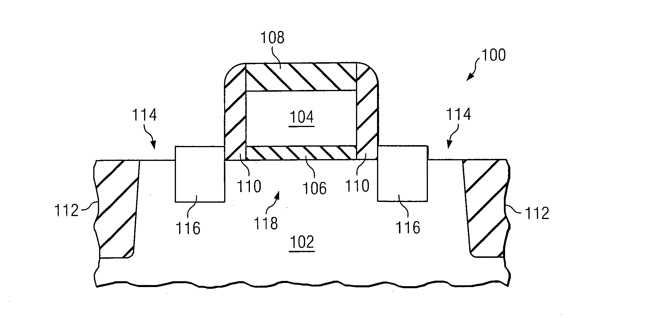
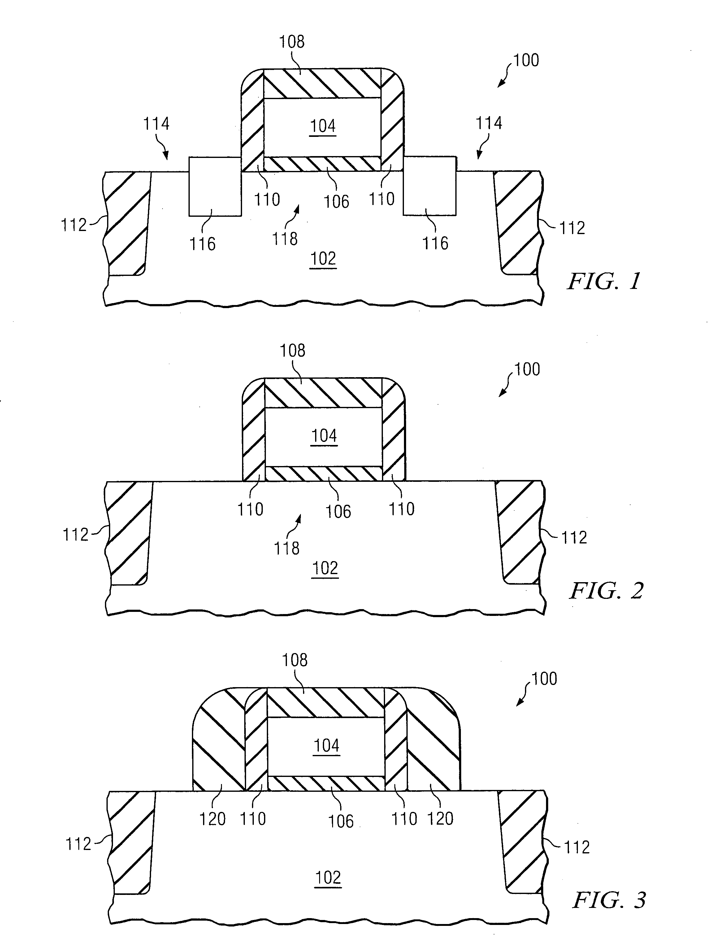
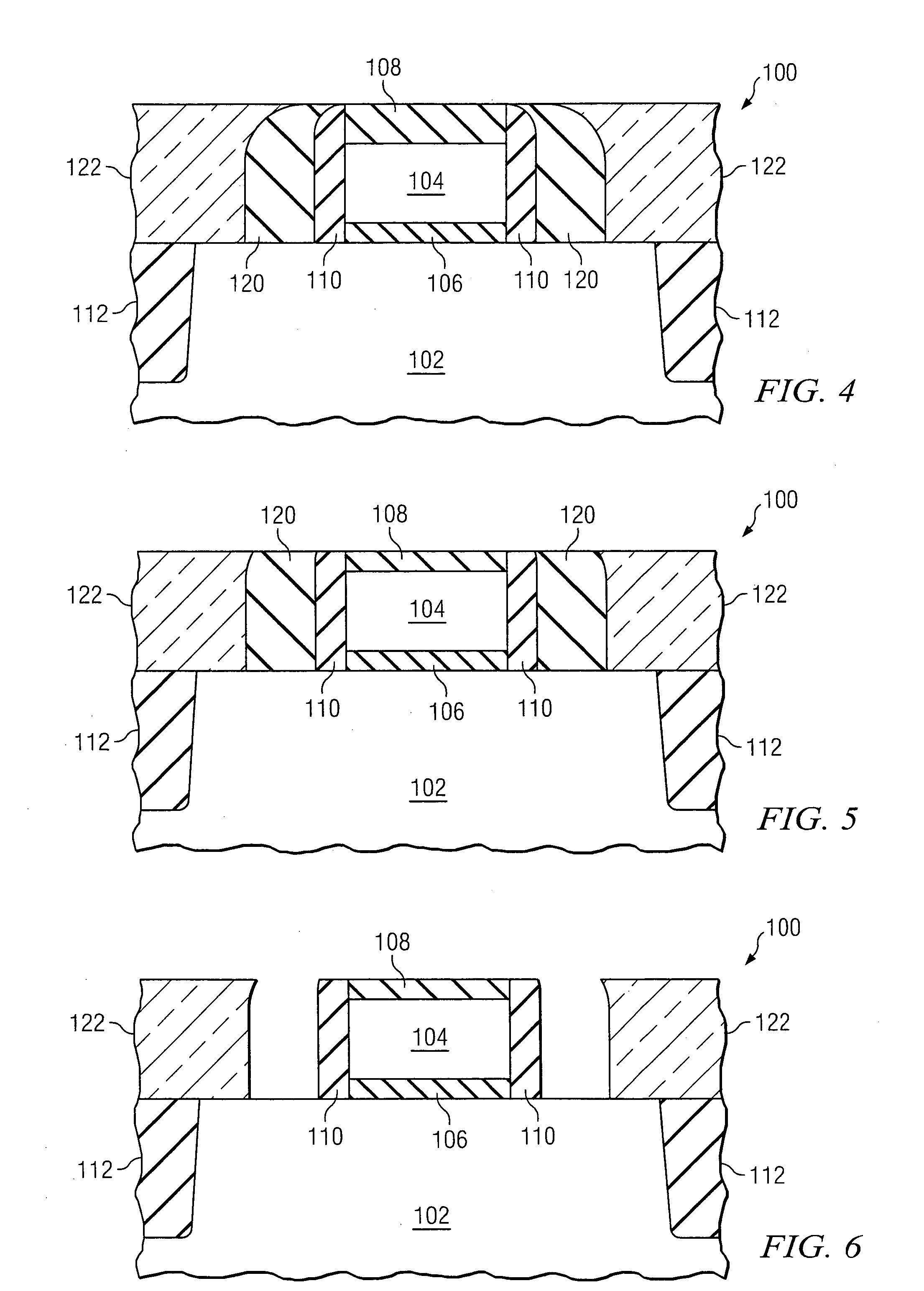
[0022]FIG. 1, illustrates a first embodiment structure 100 of the present invention that is formed in a semiconductor body 102. The semiconductor body 102 can be a bulk semiconductor substrate, a region (e....


PUM


Abstract

In a method for forming a semiconductor device, a gate electrode is formed over a semiconductor body (e.g., bulk silicon substrate or SOI layer). The gate electrode is electrically insulated from the semiconductor body. A first sidewall spacer is formed along a sidewall of the gate electrode. A sacrificial sidewall spacer is formed adjacent the first sidewall spacer. The sacrificial sidewall spacer and the first sidewall spacer overlying the semiconductor body. A planarization layer is formed over the semiconductor body such that a portion of the planarization layer is adjacent the sacrificial sidewall spacer. The sacrificial sidewall spacer can then be removed and a recess etched in the semiconductor body. The recess is substantially aligned between the first sidewall spacer and the portion of the planarization layer. A semiconductor material (e.g., SiGe or SiC) can then be formed in the recess.

Description

TECHNICAL FIELD [0001] This invention relates generally semiconductor devices and methods, and more particularly to a strained semiconductor device and a method of making the same. BACKGROUND [0002] Semiconductor devices are used in a large number of electronic devices such as computers, cell phones and others. One of the goals of the semiconductor industry is to continue shrinking the size and increasing the speed of individual devices. Smaller devices can operate at higher speeds since the physical distance between components is smaller. In addition, higher conductivity materials such as copper are replacing lower conductivity materials such as aluminum. One other challenge is to increase the mobility of semiconductor carriers such as electrons and holes. [0003] One technique to improve transistor performance is to mechanically strain (i.e., distort) the semiconductor crystal lattice near the charge-carrier channel region. Transistors built on strained silicon, for example, have g...

Claims


Application Information

Patent Timeline
Patent Type & Authority Applications(United States)
IPC IPC(8): H01L29/76H01L21/336
CPCH01L29/6653H01L29/66636H01L29/7834H01L29/7848H01L29/66477H01L21/823814H01L21/823864H01L27/1203H01L21/823807H01L27/088
Inventor TEWS, HELMUT HORSTSCHENK, ANDRE
Owner INFINEON TECH AG
Why Eureka
Try Eureka