

Electro-optical device and electronic apparatus
- Summary
- Abstract
- Description
- Claims
- Application Information
AI Technical Summary
Benefits of technology
Problems solved by technology
Method used
Image

Examples
first embodiment
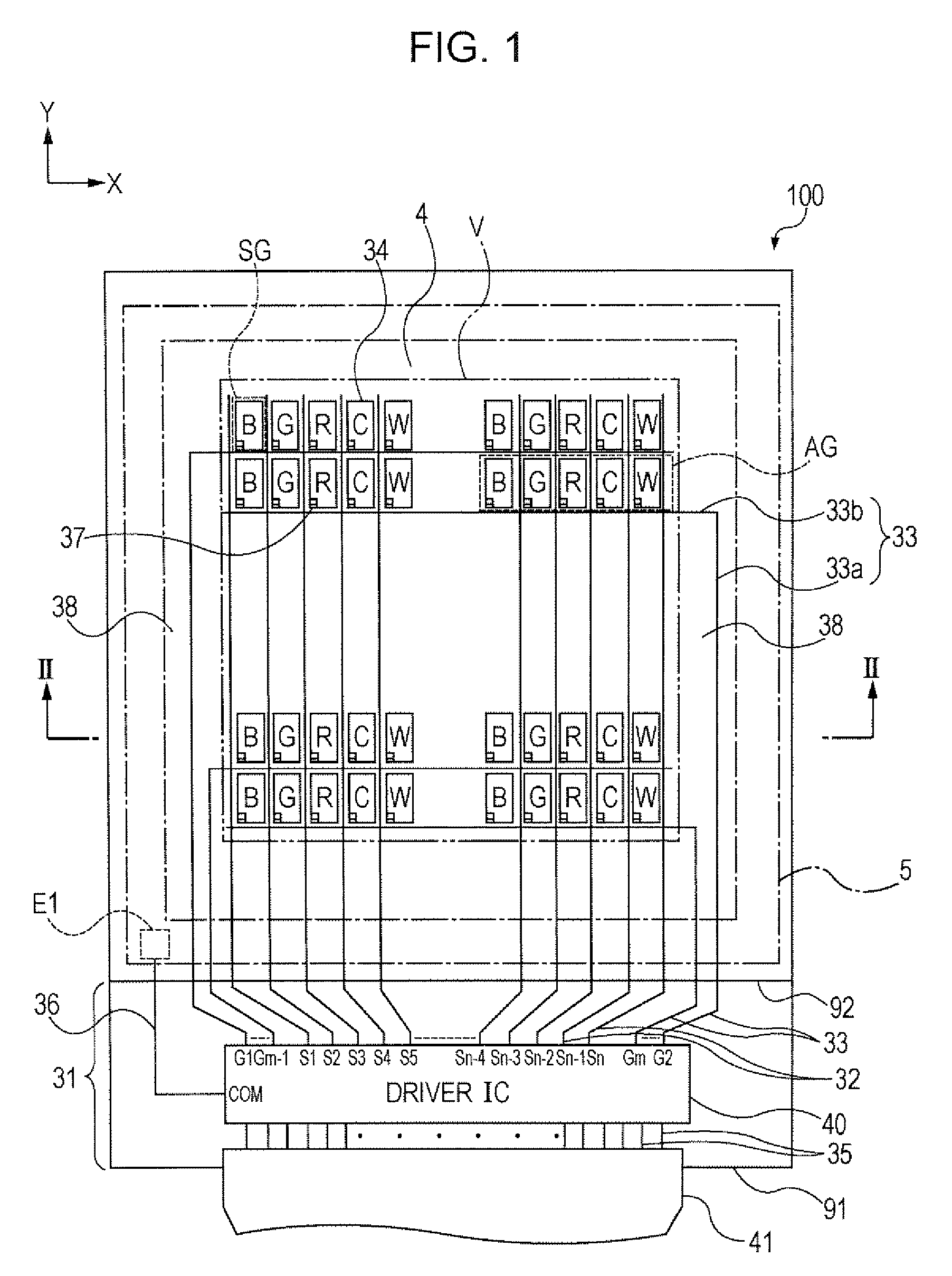
[0031] First, the structure of a liquid crystal display device 100 according to a first embodiment of the invention will be described with reference to FIGS. 1 and 2.
[0032]FIG. 1 is a plan view schematically illustrating the structure of the liquid crystal display device 100 according to the first embodiment. In FIG. 1, a color filter substrate 92 is arranged on the front surface (on the observer side) of the drawing, and an element substrate 91 is arranged on the rear side of the drawing. In FIG. 1, it is assumed that a longitudinal direction is referred to as a Y direction and a lateral direction is referred to as an X direction. In addition, in FIG. 1, R (red), G (green), B (blue), C (cyan), and W (transparent or white) regions are represented by sub-pixels SG, and a row of R, G, B, C, and W sub-pixels SG corresponds to a display pixel AG.
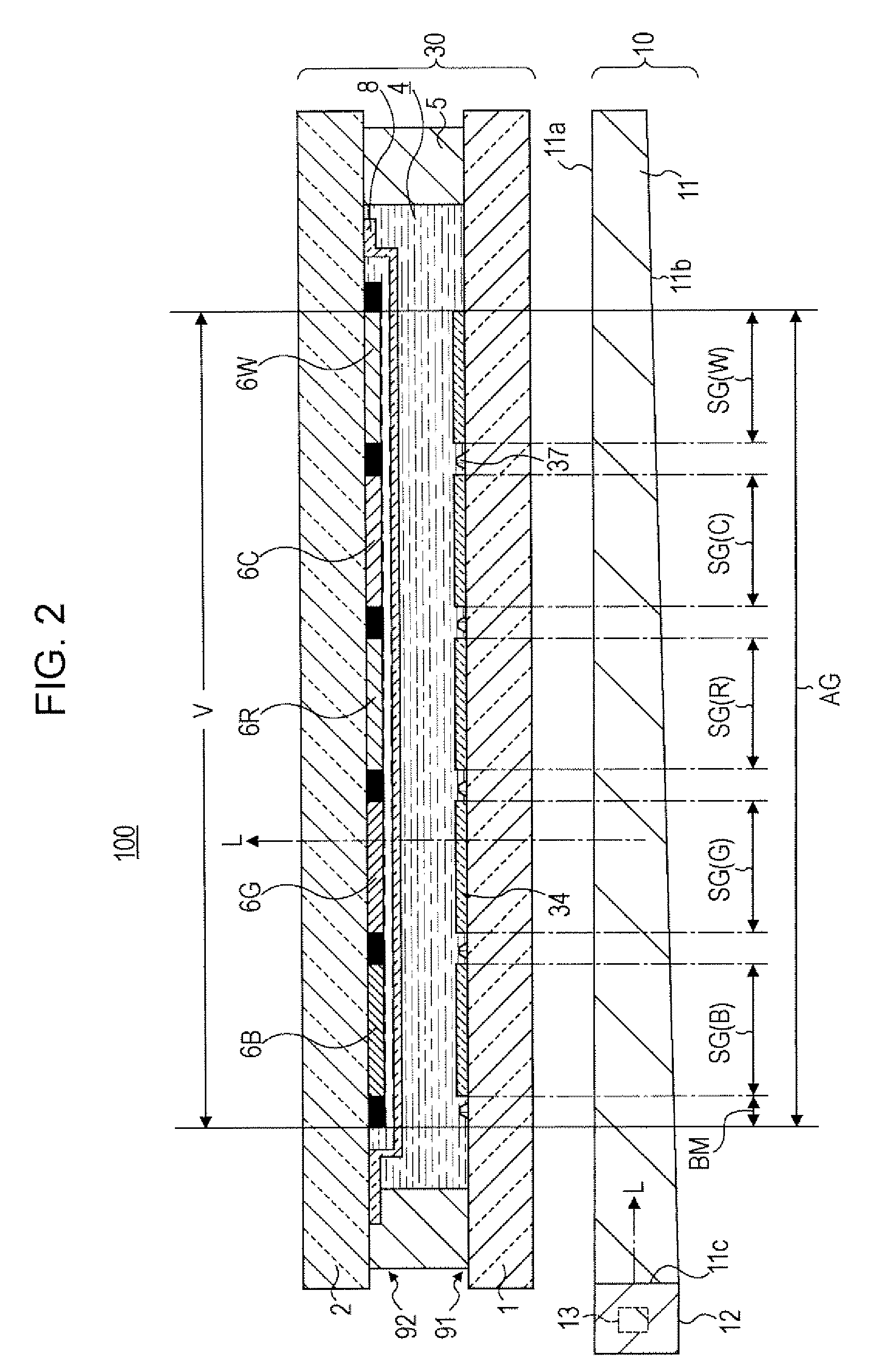
[0033]FIG. 2 is an enlarged cross-sectional view of the display pixel AG taken long the line II-II of the liquid crystal display device 100 s...
second embodiment
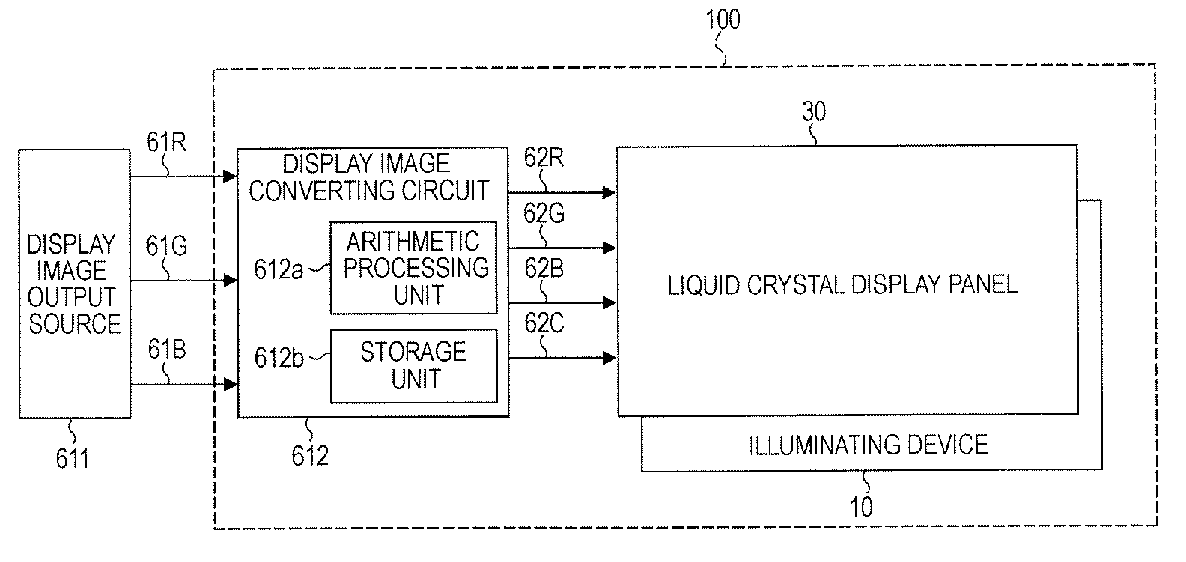
[0072] Next, a liquid crystal display device 100a according to a second embodiment of the invention will be described below. FIG. 7 is a diagram schematically illustrating the liquid crystal display device 100a according to the second embodiment. A display image converting circuit 612 of the liquid crystal display device 100a according to the second embodiment converts R, G, and B image signals output from a display image output source 611, such as a personal computer, into R, G, B, C, and W image signals, and outputs the converted image signals to a liquid crystal display panel 30.
[0073] Similar to the display image converting circuit described in the first embodiment, the display image converting circuit 612 converts R, G, and B image signals into R, G, B, and C image signals, which makes it possible to widen the color reproduction range. In this case, an arithmetic processing unit 612a calculates a brightness signal on the basis of R, G, and B signals and outputs a W image signa...
third embodiment
[0076] Next, a liquid crystal display device 100b according to a third embodiment of the invention will be described below. FIG. 8 is a diagram illustrating the liquid crystal display device 100b according to the third embodiment. The liquid crystal display device 100b according to the third embodiment differs from the liquid crystal display device 100 according to the first embodiment in that a display image converting circuit 612 supplies a control signal 62BL to an illuminating device 10. More specifically, the display image converting circuit 612 supplies the control signal 62BL to an LED 13 of the illuminating device 10 to adjust the brightness of light L emitted from a light source unit 12 of the illuminating device 10.
[0077] An arithmetic processing unit 612a of the display image converting circuit 612 determines the control signal 62BL on the basis of a brightness signal Y obtained by Expression 1. For example, when it is determined that display pixels having high brightnes...
PUM
 Abstract
Description
Claims
Application Information