Complex CMP process and fabricating methods of STI structure and interconnect structure

a technology of complex cmp and fabrication methods, applied in the direction of lapping machines, manufacturing tools, lapping apparatuses, etc., can solve the problems of inaccurate pattern transfer and high manufacturing process cost, and achieve the effects of improving polishing efficiency, reducing manufacturing cost, and increasing throughpu

Inactive Publication Date: 2007-03-22
UNITED MICROELECTRONICS CORP
View PDF2 Cites 2 Cited by
  • Summary
  • Abstract
  • Description
  • Claims
  • Application Information

AI Technical Summary

Benefits of technology

[0006] In view of the foregoing, one object of this invention is to provide a complex CMP process, which may utilize the combination of a FACMP machine and a non-fixed abrasive CMP machine for planarization to improve the polishing efficiency and thereby increase the throughput, as well as to lower the manufacturing cost.
[0007] Another object of this invention is to provide a method for fabricating an STI structure, which may use a FACMP machine together with a non-fixed abrasive CMP machine to planarize the STI insulating film for improving the polishing efficiency and the throughput of the process.
[0008] Still another object of this invention is to provide a method for fabricating an interconnect structure, which may use a FACMP machine together with a non-fixed abrasive CMP machine to planarize the conductive film for higher polishing efficiency and more throughput.
[0015] Accordingly, in a preferred embodiment of the complex CMP process of this invention, a non-fixed abrasive CMP machine is first used to coarsely polish the target film in high speed, and then a FACMP machine is used to fine polish the remaining target film with two polishing platens having substantially the same polishing rate. Therefore, not only a good planarity can be made via the fine polishing in the FACMP machine, but also the polishing time can be reduced to increase the throughput. Meanwhile, since the non-fixed abrasive CMP machine itself and the consumptive materials used therein are both cheaper, the manufacturing cost can be lowered.

Problems solved by technology

In a semiconductor process, surface planarization is a very important issue for high-resolution lithography, because a rugged surface causes significant light scattering in the exposure step making the pattern transfer inaccurate.
In addition, because the FACMP machine itself and the consumptive materials used therein are both expensive, the manufacturing process costs too much.

Method used


Image

  • Complex CMP process and fabricating methods of STI structure and interconnect structure
  • Complex CMP process and fabricating methods of STI structure and interconnect structure
  • Complex CMP process and fabricating methods of STI structure and interconnect structure

Examples


Embodiment Construction

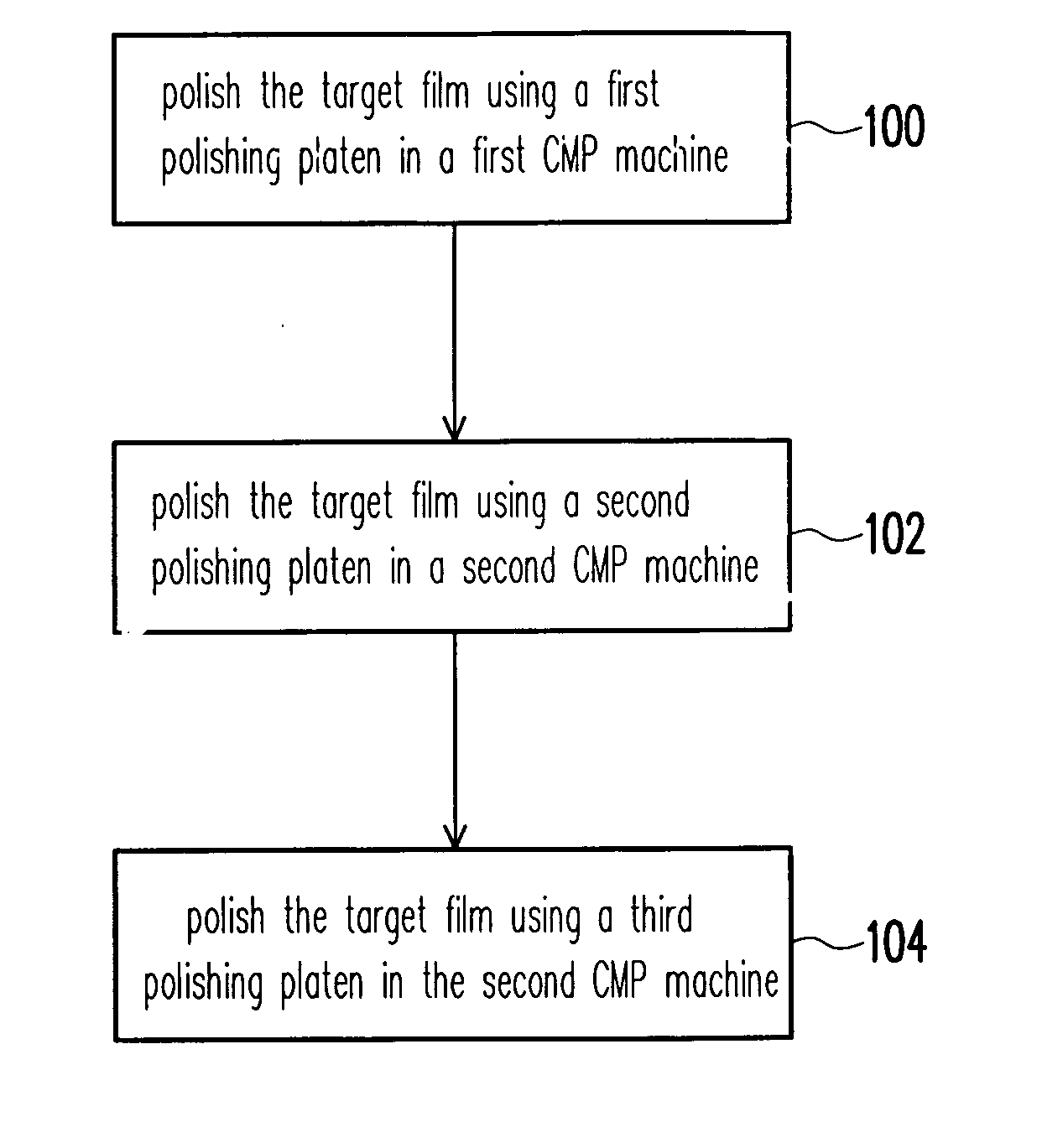
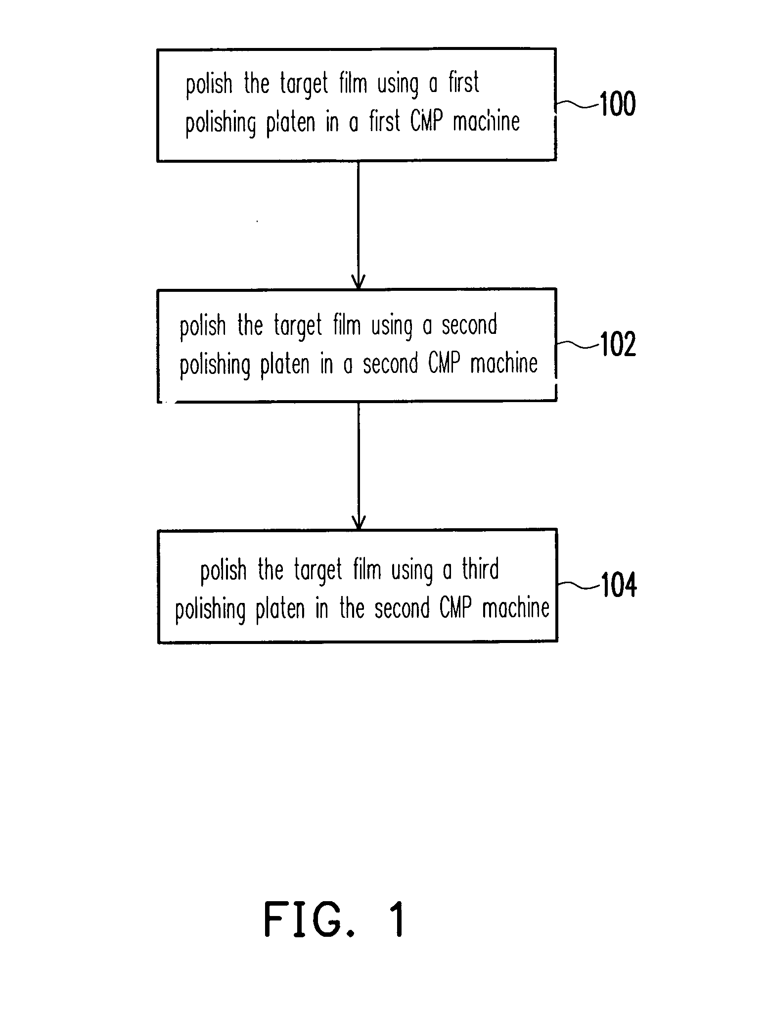
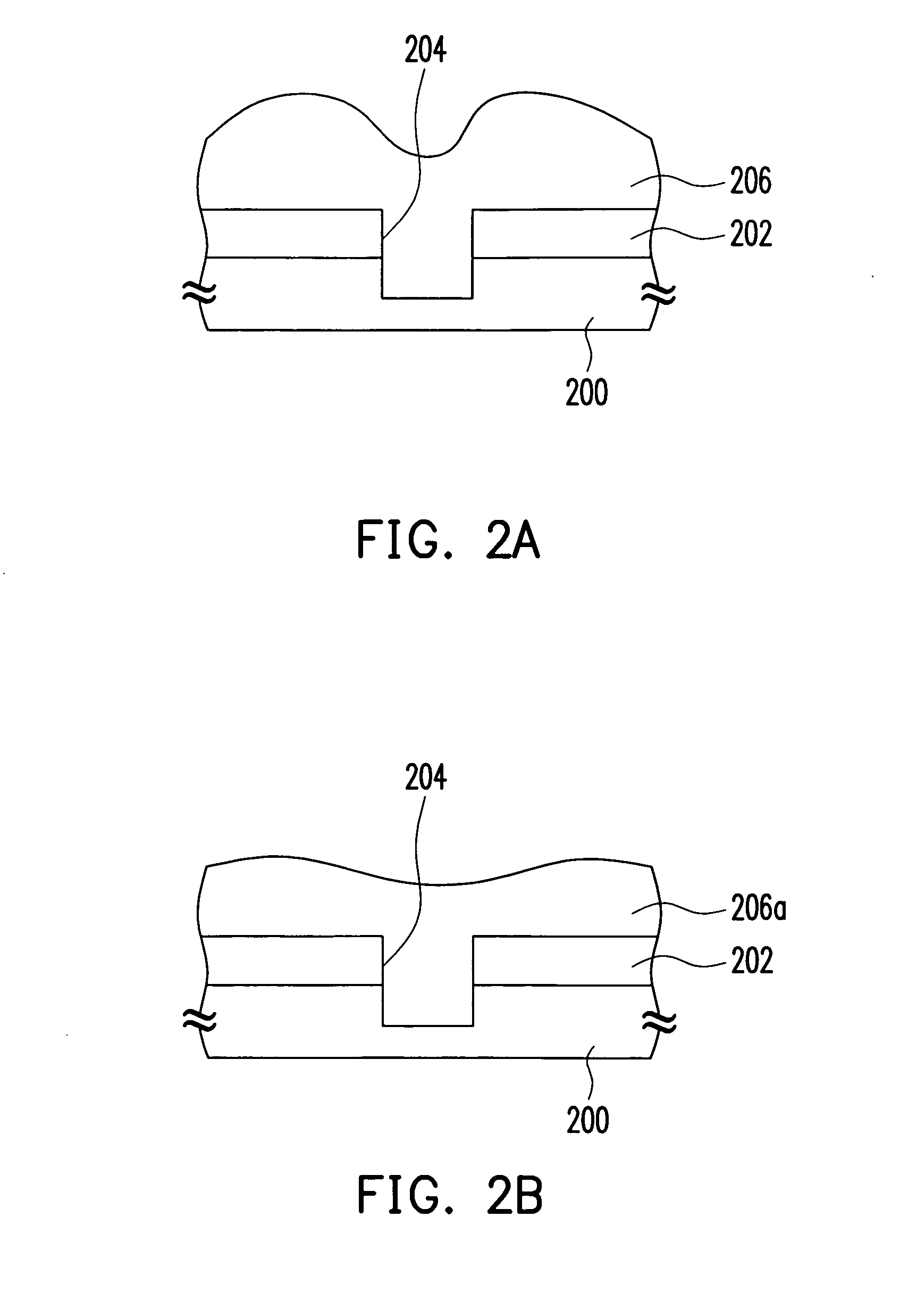
[0020]FIG. 1 illustrates the flow chart of a complex CMP process according to the preferred embodiment of this invention. In step 100, the target film, i.e., the film to be planarized, is coarsely polished using a first polishing platen in a first CMP machine that may be a non-fixed abrasive CMP machine, wherein the first polishing platen may represent one or multiple polishing platens in the first CMP machine. Specifically, in consideration of the wafer transfer mechanism in the first CMP machine, the target film can be polished using more than one polishing platens successively for improving the polishing efficiency of multiple wafers. The non-fixed abrasive CMP machine is suitable for coarse polishing in high speed, and the CMP machine itself and the consumptive materials, especially the abrasive, used therein are both cheaper so that the manufacturing cost can be lowered.

[0021] Next, the substrate having the coarsely polished target film thereon is taken out from the first CMP ...


PUM

PropertyMeasurementUnit
conductiveaaaaaaaaaa
semiconductoraaaaaaaaaa
insulatingaaaaaaaaaa

Abstract

A complex CMP process is described. A target film is coarsely polished using a first polishing platen in a first CMP machine. The remaining target film is then fine polished using successively a second polishing platen and a third polishing platen in a second CMP machine that is different from the first CMP machine.

Description

BACKGROUND OF THE INVENTION [0001] 1. Field of the Invention [0002] The present invention relates to a chemical mechanical polishing (CMP) process and fabricating methods of semiconductor structures. More particularly, the present invention relates to a complex CMP process and fabricating methods of a shallow trench isolation (STI) structure and an interconnect structure. [0003] 2. Description of the Related Art [0004] In a semiconductor process, surface planarization is a very important issue for high-resolution lithography, because a rugged surface causes significant light scattering in the exposure step making the pattern transfer inaccurate. Since the CMP technology is the only solution for global planarization in VLSI circuits and even ULSI circuits, most of wafer-surface planarization processes are currently done through CMP. [0005] Among various CMP machines, the fixed abrasive CMP (FACMP) machine is used more frequently now. A FACMP machine includes at least two polishing pl...

Claims


Application Information

Patent Timeline
Patent Type & Authority Applications(United States)
IPC IPC(8): C03C15/00H01L21/461B44C1/22C23F1/00H01L21/302
CPCB24B37/042H01L21/3212H01L21/31053
Inventor YEH, MING-HSINLEE, CHENG-CHUANCHEN, MING-TEWU, YI-CHINGHSIAO, CHIN-HSIANG
Owner UNITED MICROELECTRONICS CORP
Why Eureka
Try Eureka