Semiconductor device and semiconductor integrated circuit using the same

a technology of semiconductor integrated circuit and semiconductor, which is applied in the direction of semiconductor devices, basic electric elements, electrical appliances, etc., can solve the problems of increasing leakage current, difficult to suppress leakage current to a target value, and increasing leakage current from mos transistors, so as to improve the driving capability of mos transistors and improve processing performance. , the effect of high processing performan

Inactive Publication Date: 2007-03-22
RENESAS ELECTRONICS CORP
View PDF3 Cites 93 Cited by
  • Summary
  • Abstract
  • Description
  • Claims
  • Application Information

AI Technical Summary

Benefits of technology

[0017] Because of the configuration described above, high processing performance can be realized by driving the back gates to improve driving capability of MOS transistors. Furthermore, in the state where charging or discharging of an electric load is not being performed, a leakage current can be suppressed by driving the back gates into the reverse polarity. Thus the present invention realizes high processing performance and low power consumption.
[0018] With the present invention, semiconductor devices with high processing performance and low power consumption such as low-lower processors can be realized by suppressing an increase in circuit scale and also by reducing an increase in the area of a semiconductor chip.

Problems solved by technology

However, in the method in which a bias voltage is applied to a substrate (well), generally there is a problem in that a leakage current from the MOS transistor increases (for instance, in a case of a processor for a 3-GHz PC configured with a CMOS transistor, the leakage current ranges as high as from 20 to 30 A per chip).
In this case, since the effect is low and a leakage current due to a JN-junction is not negligible, it is difficult to suppress the leakage current to a target value.
Therefore, the method in which a back gate voltage is applied to all devices constituting the circuit is not so effective for power saving in the entire system.
Even when a voltage applied to each device is controlled independently, the circuit configuration becomes disadvantageously complicated.
In the circuit using a bulk type MOS transistor as described above, there is a problem in that a switch circuit for switching a voltage to be applied to a back gate is separately required.

Method used


Image

  • Semiconductor device and semiconductor integrated circuit using the same
  • Semiconductor device and semiconductor integrated circuit using the same
  • Semiconductor device and semiconductor integrated circuit using the same

Examples


first embodiment

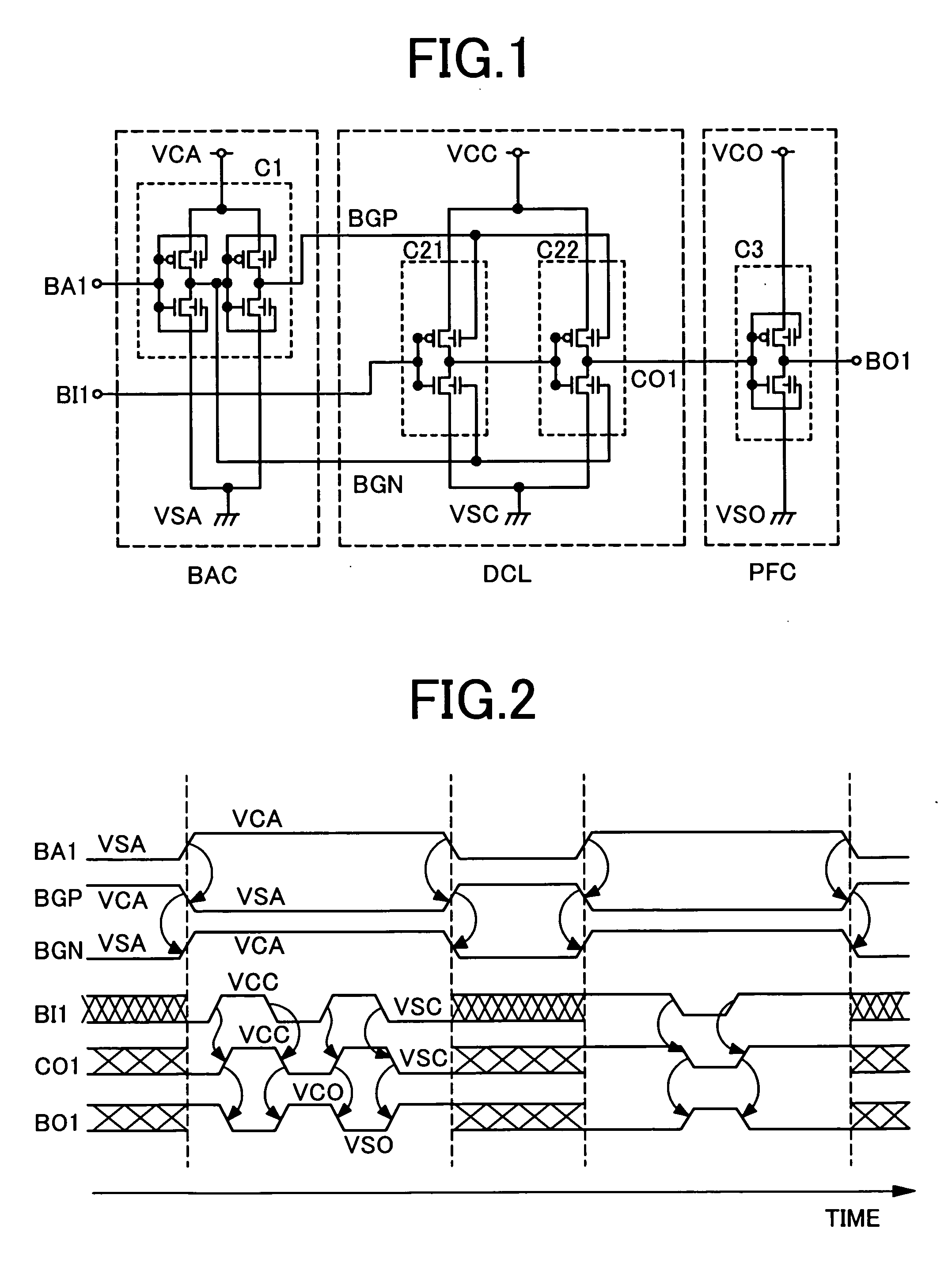
[0057]FIG. 1 illustrates a first embodiment of the present invention.

[0058] The circuit shown in FIG. 1 is largely classified to three blocks. A block DCL is a logic circuit block, a BAC block is a circuit for controlling a back gate of the Block DCL, and a PFC block is a circuit for driving an output terminal BO1 generally having a heavy load.

[0059] The DCL block is an example of a logic circuit with inverter circuits in two stages. Sign BI1 denotes an input to the DCL block and CO1 denotes an output from the DCL block. Sign VCC denotes a power voltage and sign VSC denotes the ground voltage. The signs C21 and C22 denote inverter circuits respectively, and BI1 denotes the input to the inverter circuit C21. An output from the inverter circuit C21 is provided as an input to the inverter circuit 22, and CO1 denotes an output terminal of the inverter circuit C22. In this logic circuit block DCL, namely in the two stages of inverter circuits in FIG. 1, a CMOS transistor constituting t...

second embodiment

[0078] The DCL shown in FIG. 1 is a logic circuit block as described above, and is activated by the circuit BAC and executes computing operations. Another example is shown in FIG. 7.

[0079] The DCL shown in FIG. 7 includes a NAND circuit C2 and a NOR circuit C3. In both of the circuits, back gates of each pMOS transistor are generically denoted by sign BGP, and back gates of each nMOS transistor are generically denoted by sign BGN. Generally, an input terminal for inputting a signal from outside the DCL is only the input terminal BI1. However, there may be another terminal for inputting a signal from outside the DCL. Although a terminal C2N1 and a terminal C3N1 is not shown in the figure, the terminals are connected to output terminals of other circuit in the DCL, and received signals outputted from the terminals. The block PFC includes inverters provided in two stages. Like the case shown in FIG. 1, in the blocks BAC and PFC, the gates and the back gates are connected directly.

[00...

third embodiment

[0081]FIG. 9 illustrates an example of another logic circuit used in the DCL. Signs pc, carry, s, s1, and SUM denote an input / output signal. Back gates of the pMOS transistor are connected to the BGP terminal. Back gates of each nMOS transistor are connected to the BGN terminal. In this embodiment, circuits GK are provided at some nodes in the block. The circuits GK are latch circuits for retaining signals. The latch circuit is used to stabilize a signal level at nodes connected during the standby state. In the activated state, a drive current should be weak so that a current actually driving the nodes will not be impeded.


PUM


Abstract

The present invention provides a high speed and low power consumption LSI operable in a wide temperature range in which a MOS transistor having back gates is used specifically according to operating characteristics of a circuit. In the LSI, an FD-SOI structure having an embedded oxide film layer is used and a lower semiconductor region of the embedded oxide film layer is used as a back gate. A voltage for back gates in the logic circuits having a small load in the logic circuit block is controlled in response to activation of the block from outside of the block. Transistors, in which the gate and the back gate are connected to each other, are used for the circuit generating the back gate driving signal, and logic circuits having a heavy load such as circuit block output section, and the back gates are directly controlled according to the gate input signal.

Description

CLAIM OF PRIORITY [0001] The present application claims priority from Japanese application JP 2005-222708, filed on Aug. 1, 2005, the content of which is hereby incorporated by reference into this application. BACKGROUND OF THE INVENTION [0002] 1. Field of the Invention [0003] The present invention relates to a semiconductor device requiring high speed performance and low power consumption, and more specifically to a technique which can effectively be applied to a low-lower processor circuit used in portable devices. [0004] 2. Description of the Related Art [0005] Recently there have been strong needs for increasingly higher processing performance and lower power consumption in semiconductor, especially in those such as processors. [0006] Higher processing performance of a semiconductor can generally be realized by lowering a threshold voltage. In a well-known method for lowering a threshold value, a voltage is applied to a MOS transistor substrate. In this technique, as disclosed, ...

Claims


Application Information

Patent Timeline
Patent Type & Authority Applications(United States)
IPC IPC(8): H01L27/12
CPCH01L27/1203H01L29/78648H01L29/78645H01L21/823481H01L21/823493
Inventor KAWAHARA, TAKAYUKIYAMAOKA, MASANAO
Owner RENESAS ELECTRONICS CORP
Why Eureka
Try Eureka