Organic electroluminescence element, exposure device and image forming

Inactive Publication Date: 2007-03-22
PANASONIC CORP
View PDF6 Cites 15 Cited by
  • Summary
  • Abstract
  • Description
  • Claims
  • Application Information

AI Technical Summary

Benefits of technology

[0037] Due to such a constitution, it is possible to prevent edge light of the organic electroluminescence element and, at the same time, it is possible to make the light emission brightness in the light emitting region which is restricted by the pixel restricting portion uniform. That is, the in-plane distribution (light quantity profile) of the light emission brightness of light which is radiated from the light emitting region of individual organic electroluminescence element assumes a substantially rectangular shape and hence, an exposure device which uses the organic electroluminescence element as a light source thereof can form an electrostatic latent image having a desired shape or potential distribution whereby it is possible to realize an image forming apparatus wh

Problems solved by technology

However, a voltage which is required to make the inorganic electroluminescence element emit light is high, that is, 100V or more and, further, it is difficult for the inorganic electroluminescence element to provide blue light emission and hence, it is difficult to realize a full color display using three primary colors of R, G, B. Further, in the inorganic electroluminescence element, a material which is used as a light emitting body exhibits an extremely large reflectance and hence, the light emitting body is strongly influenced by a total reflection on an interface or the like whereby a pickup efficiency of light with respect to an actual light emission into air is low, that is, 10 to 20% thus making the inorganic electroluminescence element difficult to emit light with high efficiency.
However, due to the extremely poor light emitting efficiency the full-scale studies on the practical use of the electroluminescence element have not progressed.
That is, in the above-mentioned organic electroluminescence element 11, even when the colored pixel restricting portion 18 is provided to prevent the edge light LX, the thickness of the pixel restricting portion 18 is eventually increased thus giving rise to a drawback that the light emission brightness does not become uniform in the light irradiation directions.
However, a radiation angle and a strength of the edge light LX is influenced by a delicate angle of the pixel restricting portion 18 at the end portion

Method used


Image

  • Organic electroluminescence element, exposure device and image forming
  • Organic electroluminescence element, exposure device and image forming
  • Organic electroluminescence element, exposure device and image forming

Examples


Example

Embodiment 1

[0077] Hereinafter, an embodiment 1 of the present invention is explained in conjunction with drawings.

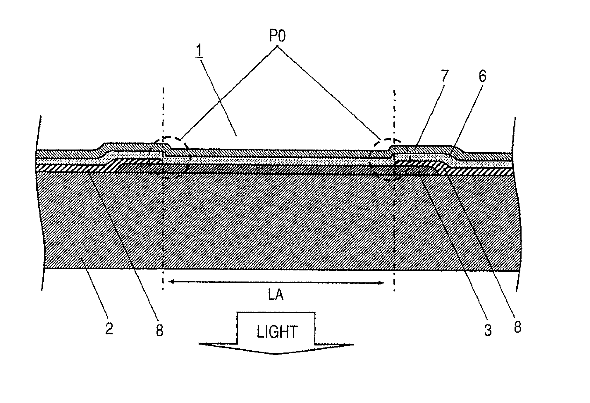
[0078]FIG. 1 is an explanatory view which shows the structure of an organic electroluminescence element 1 according to the embodiment 1 of the present invention. Hereinafter, the structure of the organic electroluminescence element 1 according to the embodiment 1 is explained in detail in conjunction with FIG. 1.

[0079] In FIG. 1, numeral 1 indicates an organic electroluminescence element according to the present invention. For the sake of brevity, for example, a drive circuit which drives an anode is omitted from FIG. 1. The circuit constitutions or the like for driving the organic electroluminescence element 1 are explained in detail later.

[0080] Numeral 2 indicates a colorless and transparent glass substrate. As the glass substrate 2, for example, it is possible to use inorganic oxide glass such as transparent or semitransparent soda ash glass, barium strontium-co...

Example

Embodiment 2

[0196]FIG. 8 is a cross-sectional view which shows the structure of the organic electroluminescence element 1 according to the embodiment 2 of the present invention. Hereinafter, although the structure of the organic electroluminescence element 1 according to the embodiment 2 is explained in detail in conjunction with FIG. 8, with respect to an exposure device which adopts the organic electroluminescence element 1 and an image forming apparatus which mounts the exposure device thereon, since there is no difference in the constitution and the operation between the embodiment 1 and the embodiment 2, the explanation thereof is omitted.

[0197] In the embodiment 2, the pixel restricting portion 8 has at least a thickness of end portion PO thereof set to a value equal to or more than 50 nm and equal to or less than 100 nm as explained in the embodiment 1 and, at the same time, a thickness of a region of the pixel restricting portion 8 other than the end portion PO of the pixe...

Example

[0213] Here, in the example 2, the explanation is made with respect t the case in which the light emitting region LA is restricted by forming the pixel restricting portion 8 with respect to the anode 3 which is formed on the glass substrate 2 in the organic electroluminescence element 1. However, it is needless to say that the technical concept of the embodiment 2 is also applicable in the same manner to the structure which restricts the light emitting region LA by forming the pixel restricting portion 8 with respect to the cathode 7 formed on the glass substrate 2.


PUM


Abstract

In an organic electroluminescence element, a stray light which is confined in the inside of a light emitting layer, an anode and a glass substrate receives the conversion of angle at an end portion of a pixel restricting portion and is eradiated and hence, a substantial light emitting region is expanded from an original light emitting region. When such an organic electroluminescence element is used in an exposure device, the resolution is substantially lowered. To overcome such a drawback, the present invention provides an organic electroluminescence element includes an anode to which holes are injected, a light emitting layer, a cathode to which electrons are injected, and a pixel restricting portion which restricts a light emitting region of the light emitting layer by controlling the injection of at least one of the holes and the electrons, wherein a thickness of an end portion of the pixel restricting portion on a side thereof which restricts the light emitting region is set to a value equal to or more than 20 nm and equal to or less than 100 nm.

Description

BACKGROUND OF THE INVENTION [0001] 1. Field of the Invention [0002] The present invention relates to an organic electroluminescence element, an exposure device which uses the organic electroluminescence elements in a row thus forming an exposure light source, and an image forming apparatus which mounts the exposure device thereon. [0003] 2. Description of the Related Art [0004] The electroluminescence element is a light emitting device which makes use of an electric field light emission of a solid fluorescent material. Currently, an inorganic electroluminescence element which uses an inorganic material as a light emitting body has been put into practice and the inorganic electroluminescence element has been partially applied to a backlight of a liquid crystal display or a flat display. However, a voltage which is required to make the inorganic electroluminescence element emit light is high, that is, 100V or more and, further, it is difficult for the inorganic electroluminescence ele...

Claims


Application Information

Patent Timeline
IPC IPC(8): H01J1/62H01J63/04
CPCH01L51/5262H01L27/3246H10K59/122H10K50/85
Inventor HAMANO, TAKAFUMIYAMAMOTO, SHINYA
Owner PANASONIC CORP
Why Eureka
Try Eureka