Liquid crystal display on a printed circuit board

a printed circuit board and liquid crystal display technology, applied in static indicating devices, non-linear optics, instruments, etc., can solve the problems of complicated, fragile and problematic components, difficult interconnection, and laborious interconnections between drive electronics and display cells, and achieve simplified lcd manufacturing processes and lower costs.

Inactive Publication Date: 2007-03-22
KENT DISPLAY SYST
View PDF99 Cites 65 Cited by
  • Summary
  • Abstract
  • Description
  • Claims
  • Application Information

AI Technical Summary

Benefits of technology

[0010] The advantages of the invention are: simplified LCD manufacturing processes vs. currently produced displays; lower cost; a much more rugged display; and the ability to create borderless display panels which can be tiled together into a large format display matrix. Fragile interconnection cables / tabs are eliminated from the display and existing manufacturing technologies are employed; printing, screening, coating.

Problems solved by technology

Interconnects between the drive electronics and the display cell are one of the most labor intensive, intricate, fragile and problematic components of a flat panel display and its manufacturing.
More recently, efforts to construct displays on flexible substrates such as plastic have made the interconnect issue more problematic than ever in that interconnects must also be flexible if the same construction designs are employed that were used on glass displays.

Method used


Image

  • Liquid crystal display on a printed circuit board
  • Liquid crystal display on a printed circuit board
  • Liquid crystal display on a printed circuit board

Examples


example 1

[0037] An operable 13×16 pixel passive matrix cholesteric display was made by coating and printing the various display elements on a plastic substrate with back pressure sensitive adhesive (PSA) layer and release liner. The plastic substrate was a PET sheet with a thickness of 12.5 microns available from Grafix (Cleveland). A layer of conducting polymer (ELP-3040 available from Agfa-Gevaert, Belgium) was screen printed on the plastic substrate as 5 mm wide, 15 cm long electrode strips spaced 1 mm apart to serve as the column electrodes of the passive matrix display. After casting, the conducting polymer was cured at 100° C. for 10 minutes. A layer of encapsulated cholesteric liquid crystal in polymer binder was coated from a water-based emulsion on the conducting polymer layer using a doctor blade having a 25 micron (μm) gap and allowed to dry for 1 hour at room temperature. The thickness of the encapsulated liquid crystal layer was approximately 8-10 μm. The emulsion was prepared f...

example 2

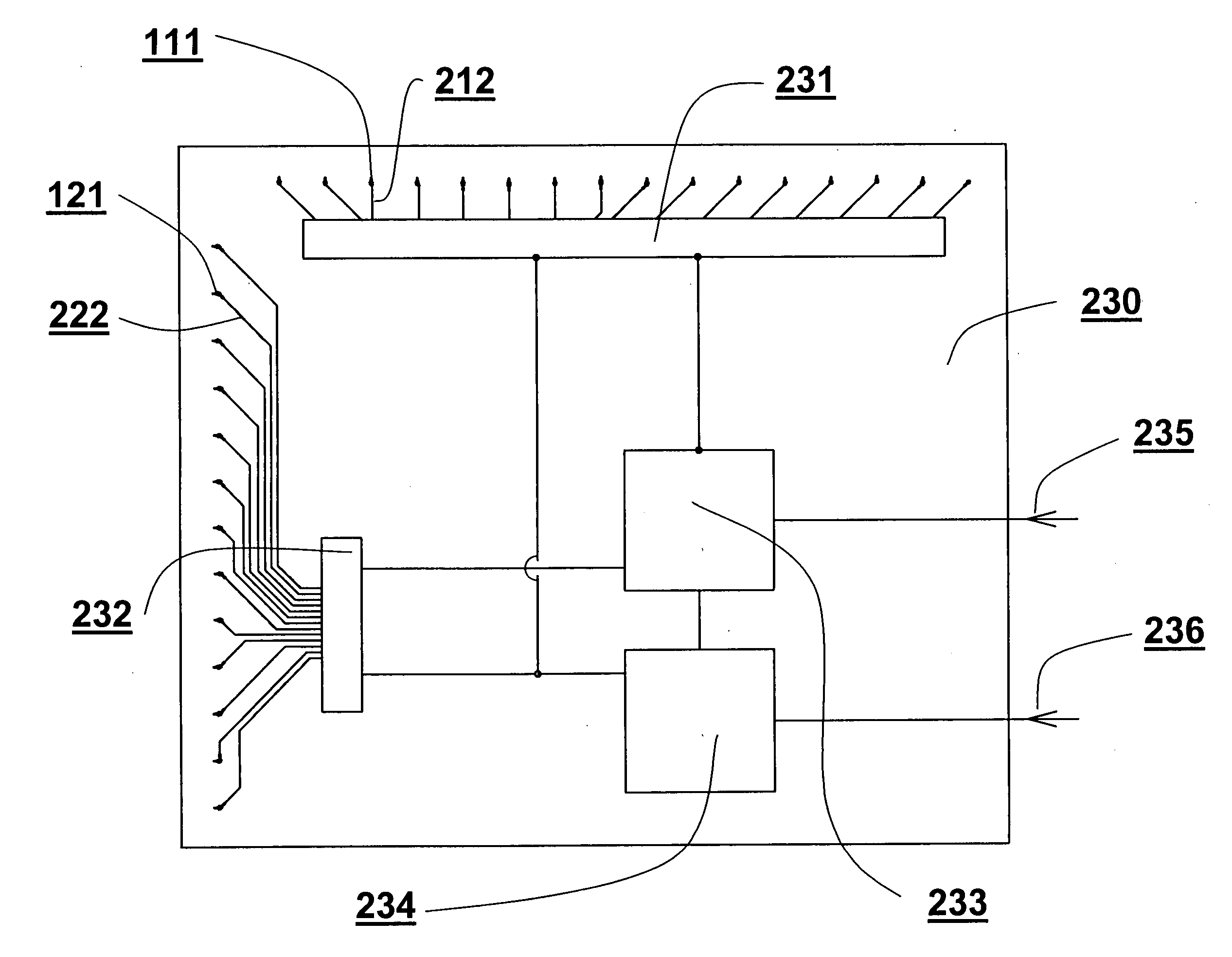
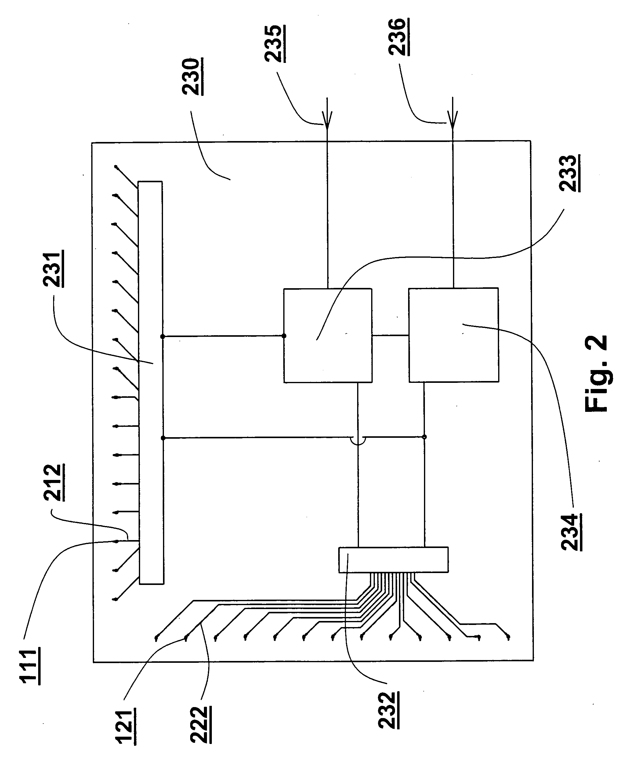
[0039] The following is an example of preparation of the coated cholesteric display directly on the PCB. The display had the same sequence of layers as in Example 1 except that the 12.5 μm PET with PSA and release liner were replaced by the PCB. All display layers including bottom conducting polymer electrodes, encapsulated liquid crystal, top conducting polymer electrodes and clear coat were sequentially coated directly on the PCB as a substrate.

[0040] The top conducting polymer electrodes were connected to the PCB pads as in Example 1. The bottom conducting polymer electrodes were connected to the driving electronics through vias in the PCB.


PUM


Abstract

The present invention features a liquid crystal display device including a printed circuit board, PCB, substrate composed of non-conductive material and having a front surface and having an opposing back surface that contains electrical circuitry and is located near the back of the display device. A liquid crystal display is disposed on the front PCB substrate surface and includes first and second electrode layers and a dispersion layer disposed between the first and second electrode layers. The dispersion layer includes liquid crystal (e.g., cholesteric liquid crystal) dispersed in a polymer matrix. Electrical through-conductors extend between the front substrate surface and the back substrate surface. The through-conductors are in electrical contact with the first and second electrode layers. Drive electronics are disposed on the PCB substrate and are adapted to apply voltage pulses to the first and second electrodes effective to form images on the liquid crystal display. In one aspect the front of the PCB substrate is a non-component surface free of drive electronics. In another aspect, the PCB substrate is the only substrate of the display device. Also featured are methods of making the display device, including forming the display as a transfer film, which forms an electrical connection when the first electrode layer is applied to the PCB substrate. Another method forms the device by printing or coating the display component layers on the PCB substrate.

Description

I. FIELD OF THE INVENTION [0001] The present invention is directed to the field of liquid crystal displays and, in particular, to flexible liquid crystal displays. II. BACKGROUND OF THE INVENTION [0002] Flat panel displays as they appear in the marketplace today are generally all constructed on glass substrates. Liquid crystal displays (LCDs) that hold the greatest market share are fabricated using two glass substrates with liquid crystalline material sandwiched in between. In recent years there has been considerable interest in fabricating LCDs as well as other technologies on substrates that are flexible such as plastic or even drapable such as fabric. Such substrates are not so easily broken, are lighter in weight, and can be flexed, bent or made conformable to specific shapes and hold potential for lower cost roll-to-roll or sheet-to-sheet manufacturing. [0003] In most of the LCD examples above, the bulk of the drive and control electronic circuitry is on a printed circuit board...

Claims


Application Information

Patent Timeline
Patent Type & Authority Applications(United States)
IPC IPC(8): G09G3/36
CPCG02F1/13452G02F1/1347G02F1/13718G09G2300/0426G09G3/3629G09G2300/0408G09G3/3611
Inventor BELLAMY, ALAN KEITH
Owner KENT DISPLAY SYST
Why Eureka
Try Eureka