

Solid state imaging device, driving method for solid state imaging device, imaging apparatus, and image input apparatus
a driving method and imaging device technology, applied in the direction of television systems, radioation controlled devices, instruments, etc., can solve the problems of deteriorating device reliability, reducing the pinning effect, and deteriorating the transfer efficiency of the vertical transfer register, so as to improve the reliability of the device, reduce the transfer efficiency, and improve the transfer efficiency
- Summary
- Abstract
- Description
- Claims
- Application Information
AI Technical Summary
Benefits of technology
Problems solved by technology
Method used
Image

Examples
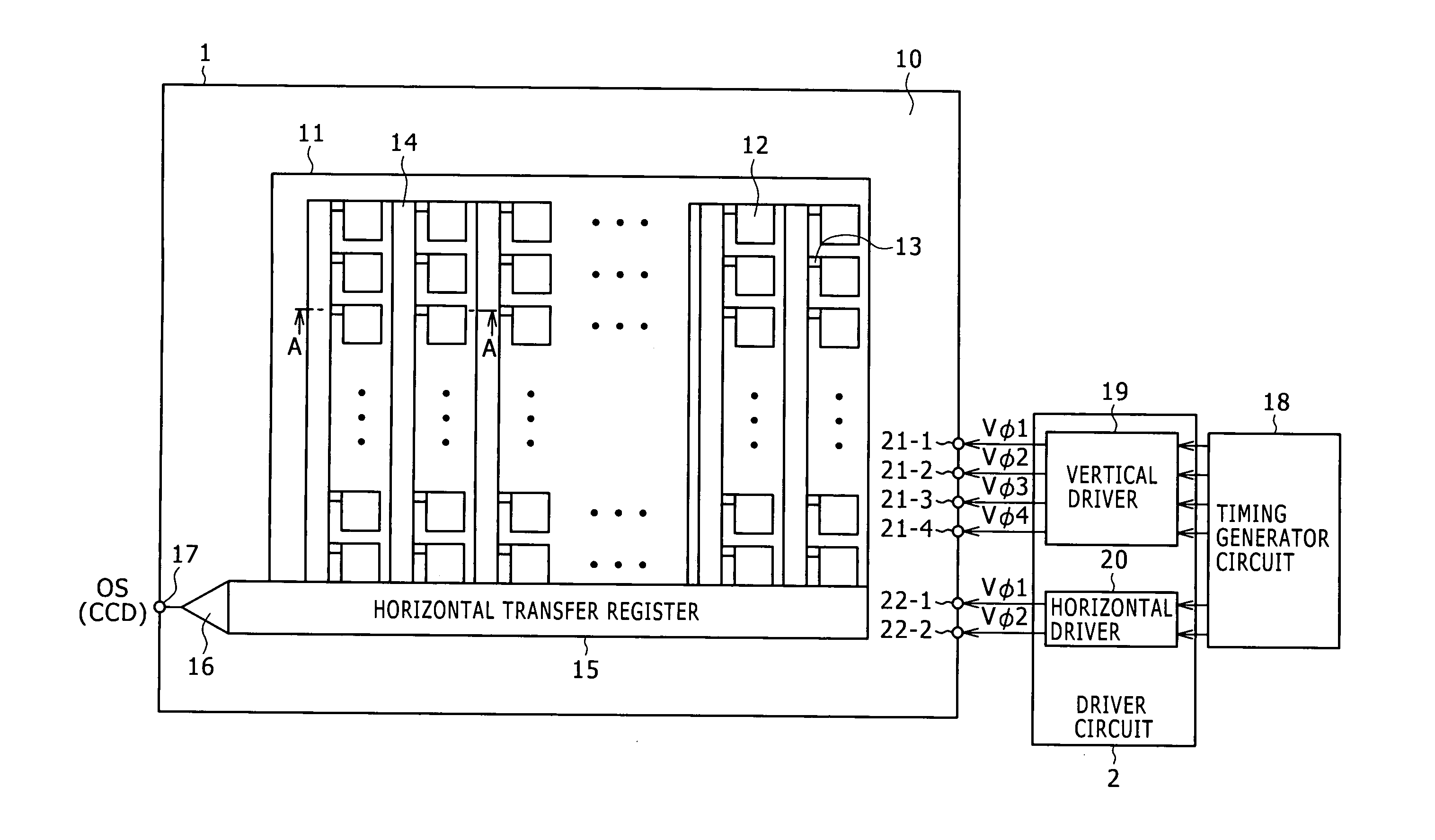
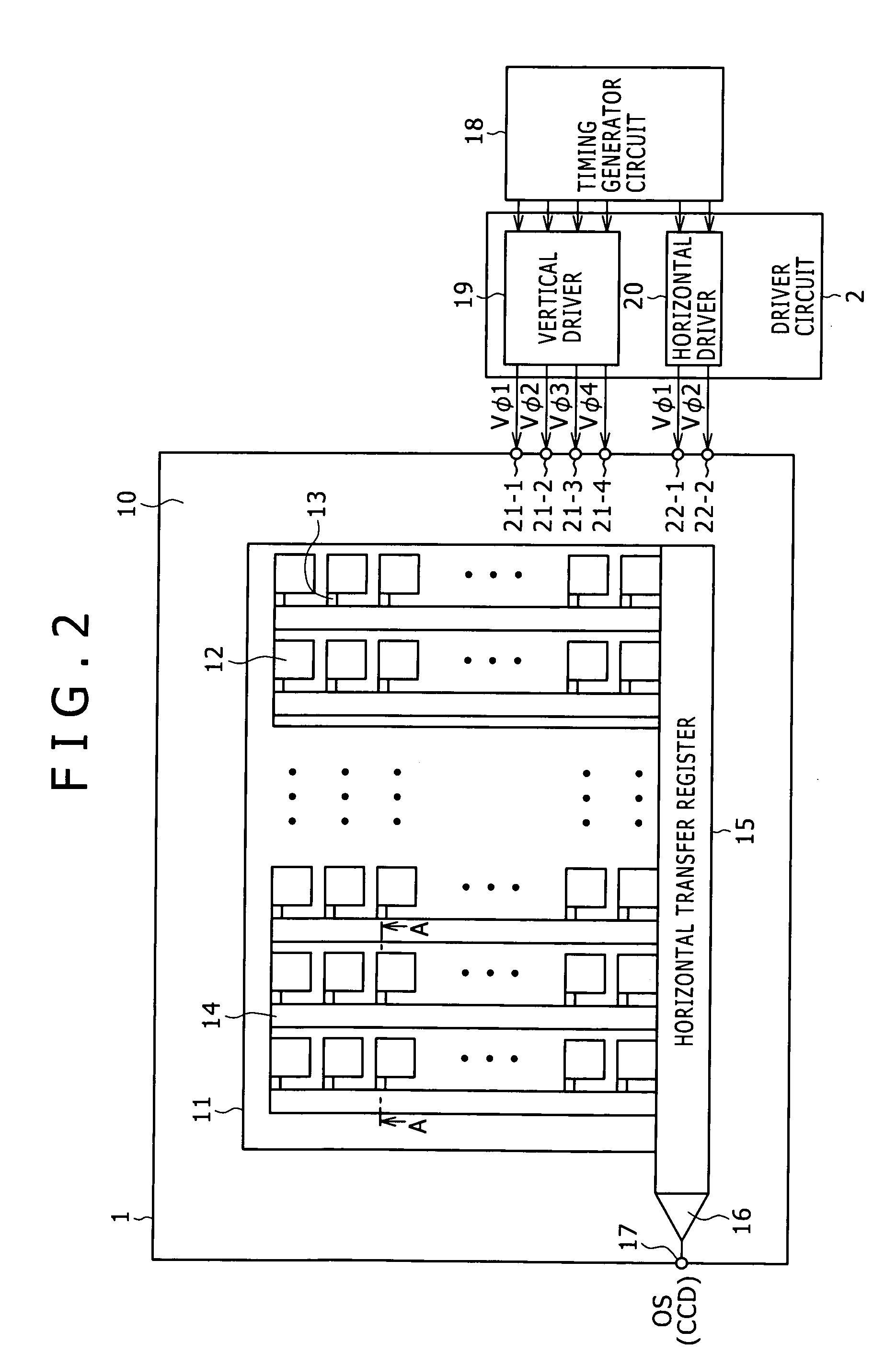
first embodiment
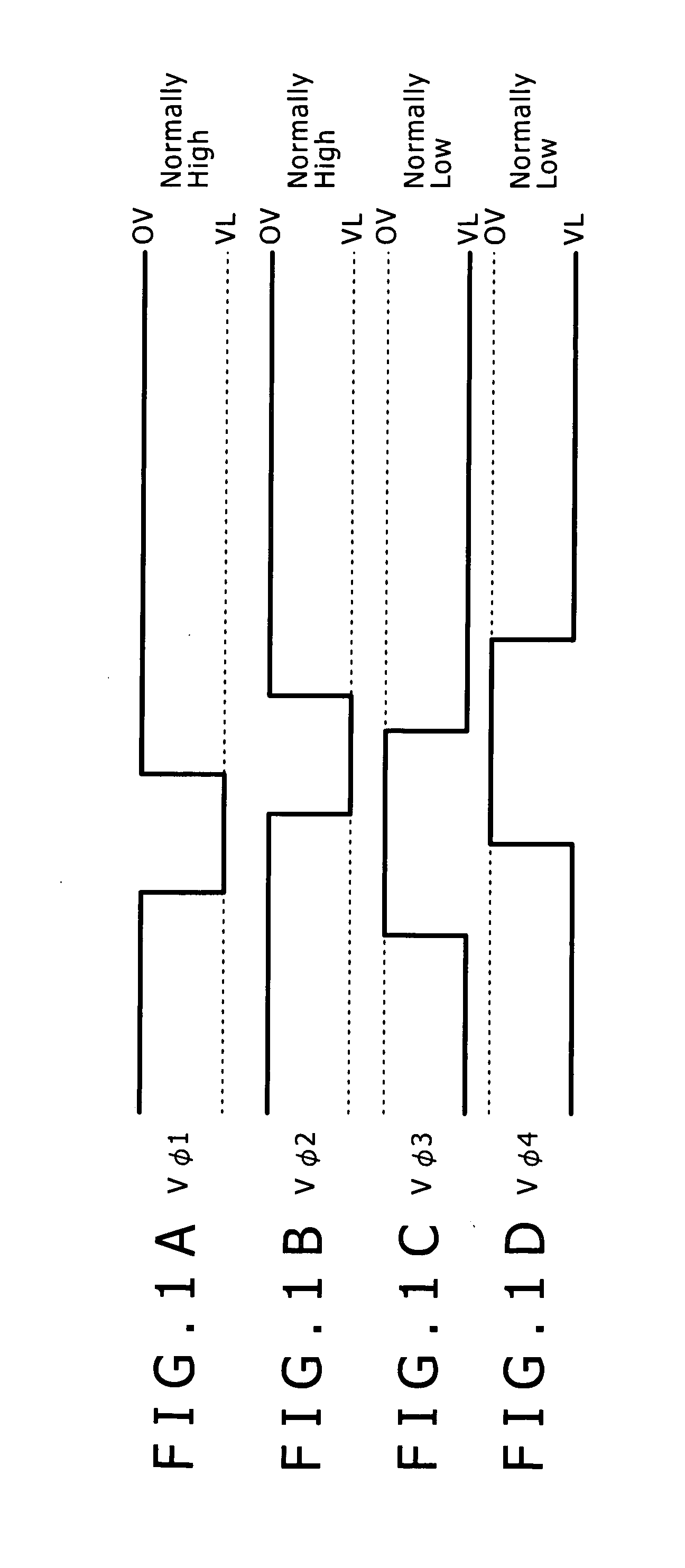
[0075]FIG. 4A to 4D, respectively, are waveform diagrams of four phase-differential vertical transfer pulse trains according to the first embodiment. Referring to the drawing figures, the four phase-differential vertical transfer pulse trains (Vφ1 to Vφ4) are composed of normally high transfer pulses (normally high vertical transfer pulses Vφ1 and Vφ2 in the present embodiment) that each have a longer duration of the positive side potential (0 V in the present embodiment) than a duration of the negative side potential (negative voltage value VL in the present embodiment), and normally low transfer pulses (vertical transfer pulses Vφ3 and Vφ4 in the present embodiment) that each have a longer duration of the negative side potential than the duration of the positive side potential.
[0076] In the first embodiment, a feature is that a negative side potential VL′ of the normally low vertical transfer pulse Vφ3, Vφ4 is set smaller in absolute value than the negative side potential VL of t...
second embodiment
[0099] In the present (second) embodiment, level variations of transfer pulses are intermittently effected. FIGS. 2 and 3 are commonly applied as well to the present embodiment.
[0100]FIG. 5A to 5D, respectively, are waveform diagrams of four phase-differential vertical transfer pulse trains according to the second embodiment.
[0101] Referring to the drawing figures, similarly as in the case of the first embodiment, the four phase-differential vertical transfer pulse trains (Vφ1 to Vφ4) are composed of normally high vertical transfer pulses Vφ1 and Vφ2 that each have a longer duration of the positive side potential (0[V] in the present embodiment) than the duration of the negative side potential (negative voltage value VL in the present embodiment), and normally low transfer pulses Vφ3 and Vφ4 that each have a longer duration of the negative side potential than the duration of the positive side potential.
[0102] In the second embodiment, a feature is that a negative side potential V...
application example
[0113] The CCD solid state imaging device of the respective embodiment described above is well suited for use as an imaging device of any one of imaging apparatuses, such as a digital still camera and a video camera.
[0114] In the present example case, the imaging apparatus refers to a camera module (used by being mounted in an electronic apparatus, such as a mobile phone) or a camera system, such as a digital still camera or video camera, including the camera module. The camera module includes a solid state imaging device serving as an imaging device, an optical system for imaging image light of a photographic subject onto an imaging surface (light reception surface) of the solid state imaging device, and a signal processing circuit of the solid state imaging device.
[0115]FIG. 10 is a block diagram of an example of the configuration of the image input apparatus in the embodiment according to the present invention. Referring to FIG. 10, the imaging apparatus of the present example ...
PUM
 Abstract
Description
Claims
Application Information