

Photomask and pattern formation method and mask data generation method using the same
a pattern formation and mask technology, applied in the field of photomask and pattern formation method and mask data generation method using the same, can solve the problem of difficult to increase the process margin in exposure using a photomask, and achieve the effect of improving the contrast in the light intensity distribution and increasing the process margin
- Summary
- Abstract
- Description
- Claims
- Application Information
AI Technical Summary
Benefits of technology
Problems solved by technology
Method used
Image

Examples
embodiment 1
[0091] A photomask according to Embodiment 1 of the invention will now be described with reference to the accompanying drawings.
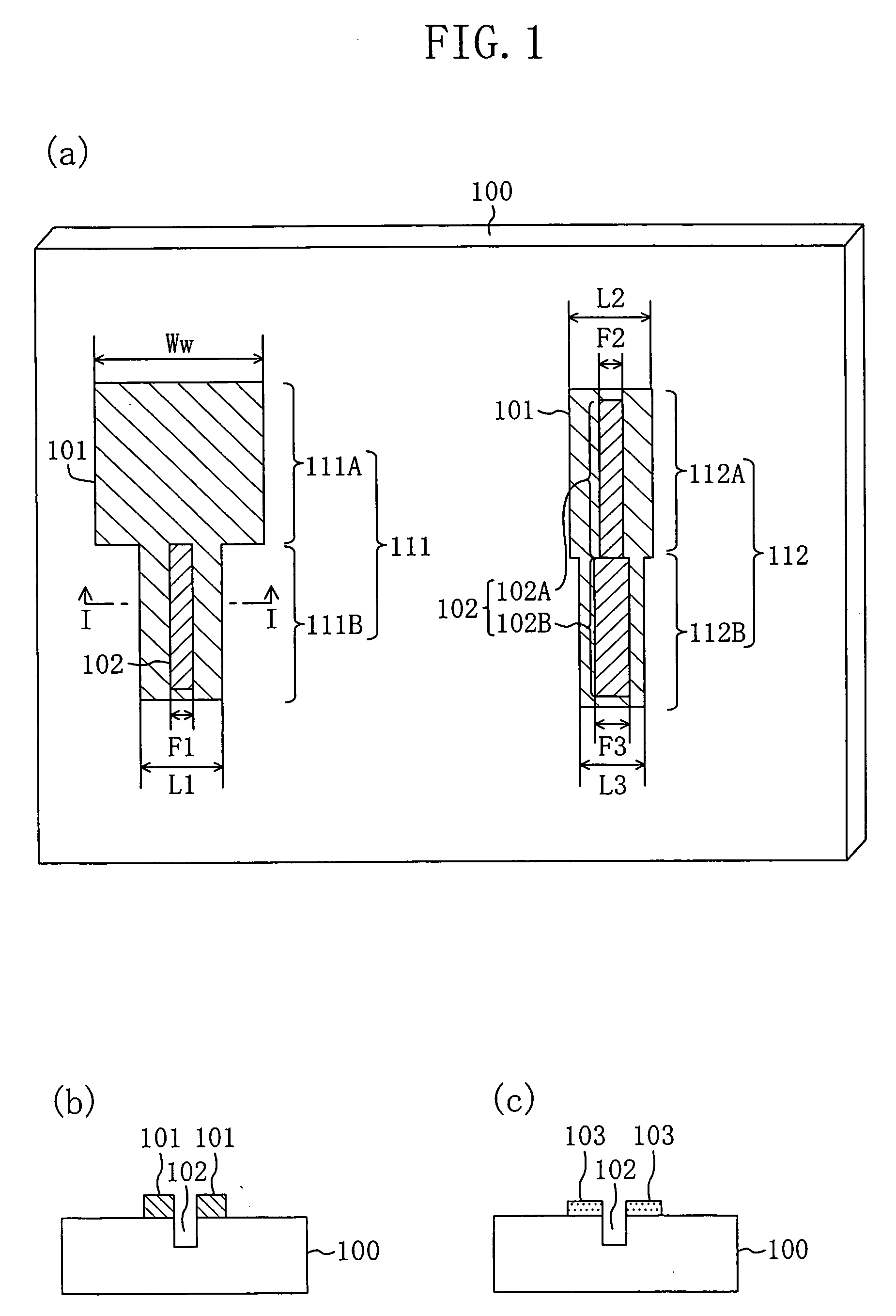
[0092]FIG. 3A is a plan view of the photomask of Embodiment 1 and FIG. 3B is a cross-sectional view taken on line II-II of FIG. 3A. It is noted that a transparent substrate 100 is perspectively shown in FIG. 3A.
[0093] As shown in FIG. 3A, mask patterns (line patterns 121 through 123) used for forming desired line-shaped patterns on a wafer through exposure are drawn on the transparent substrate 100. At this point, each of the line patterns 121 through 123 is basically made of a shielding portion 101. Also, in a central portion of a pattern region with a line width not larger than a given dimension W0 in each of the line patterns 121 through 123, the shielding portion 101 has an opening in which a phase shifter 102 is provided. In other words, each of the line patterns 121 through 123 has the mask enhancer structure. For example, the pattern 121 is a patte...
modification 1
of Embodiment 1
[0133] A photomask according to Modification 1 of Embodiment 1 of the invention will now be described with reference to the accompanying drawings.
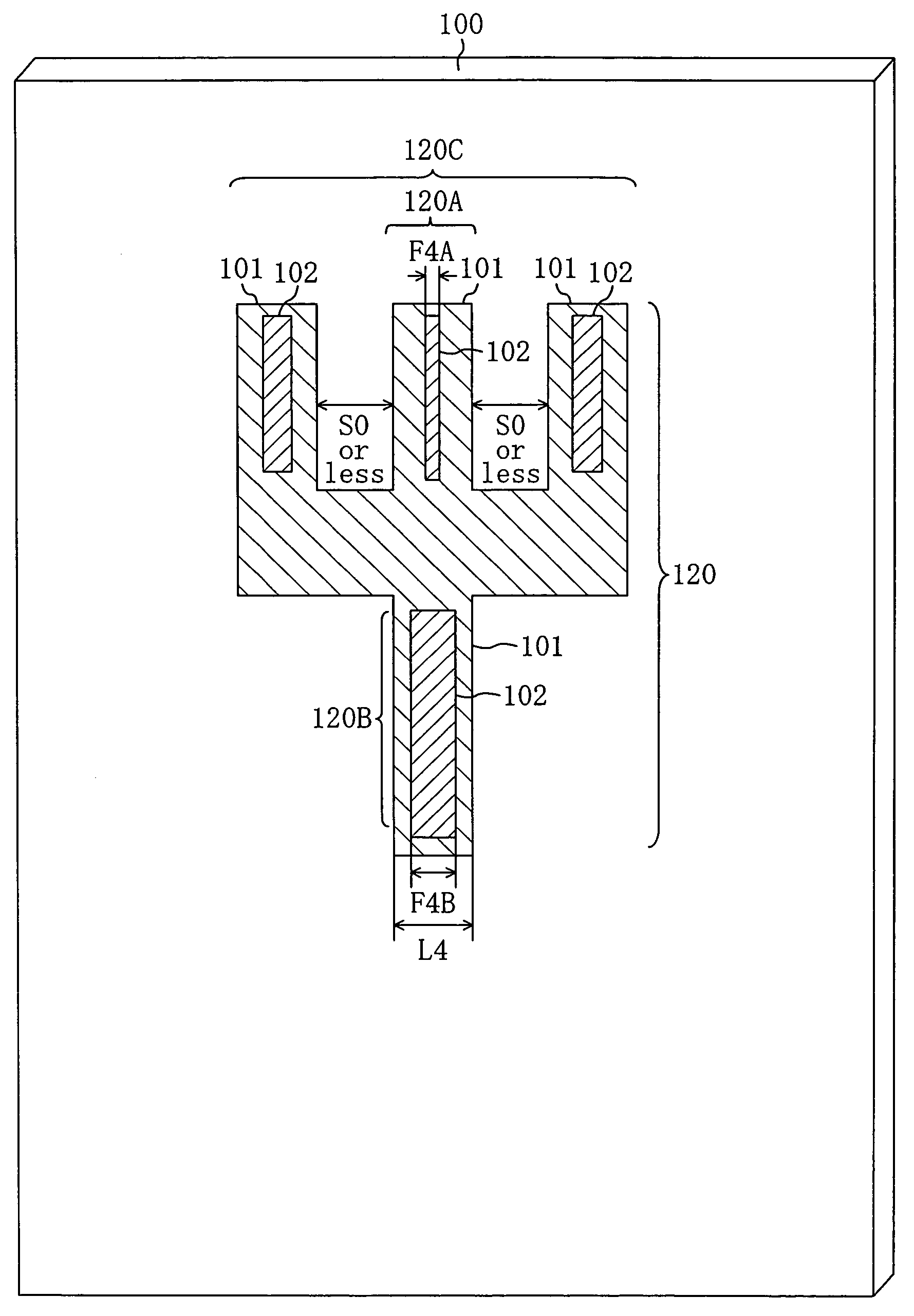
[0134]FIG. 11 is a plan view of the photomask of Modification 1 of Embodiment 1, and more specifically, a photomask provided with a mask pattern having the mask enhancer structure and included in densely arranged patterns. In FIG. 11, a transparent substrate 100 is perspectively shown.
[0135] As shown in FIG. 11, mask patterns (line patterns 124 through 128) for forming desired line-shaped patterns on a wafer through exposure are drawn on the transparent substrate 100. In this case, each of the line patterns 124 through 128 is basically made of a shielding portion 101. Furthermore, a phase shifter 102 is provided at the center of a pattern region of each of the line patterns 124 through 128 having a line width not larger than a given dimension WO. Specifically, each of the line patterns 124 through 128 has the mask enhancer...
modification 2
of Embodiment 1
[0154] A photomask according to Modification 2 of Embodiment 1 of the invention will now be described with reference to the accompanying drawings.
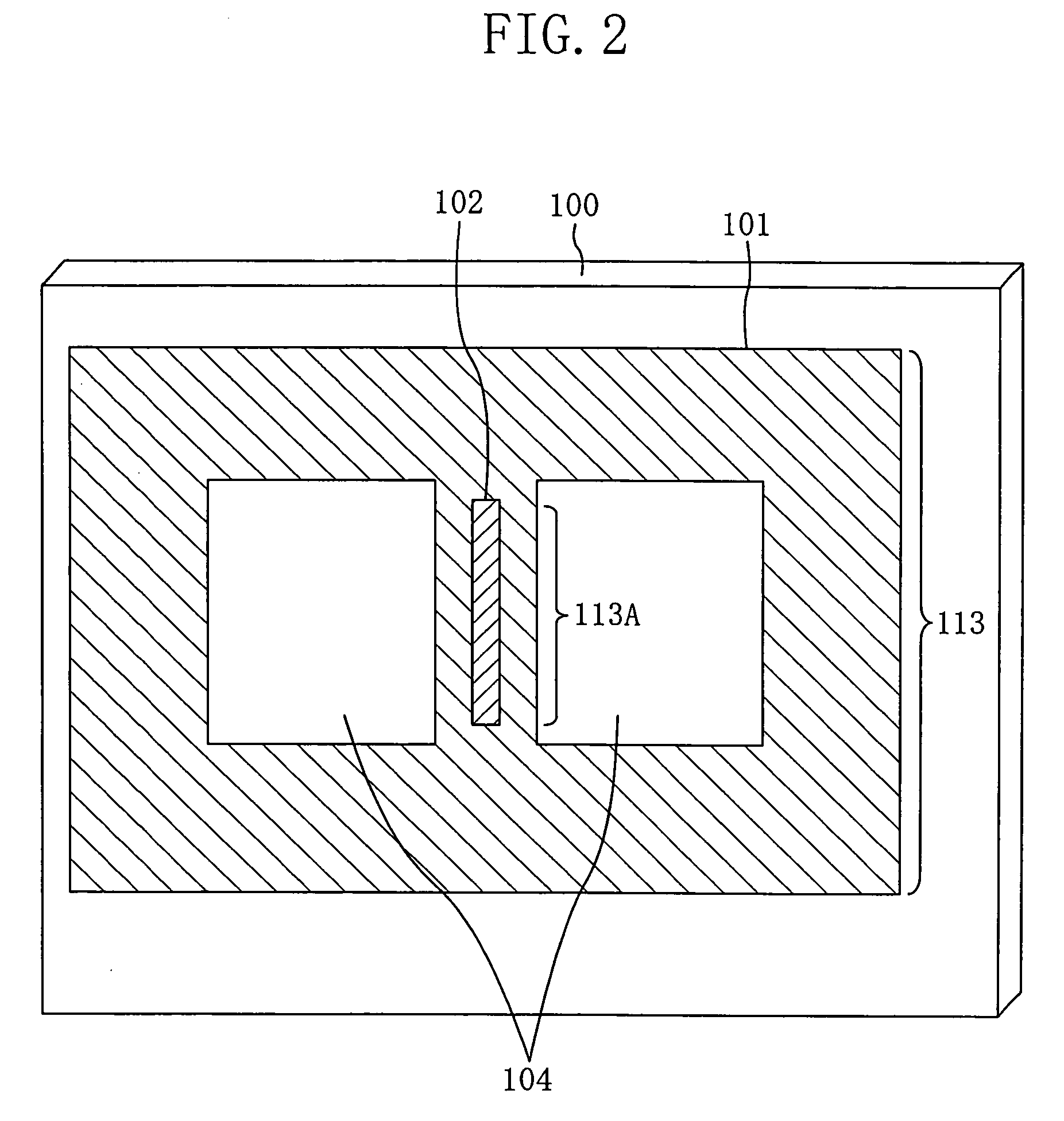
[0155]FIG. 14 is a plan view of the photomask of Modification 2 of Embodiment 1, and more specifically, a photomask provided with a mask pattern having the mask enhancer structure and included in densely arranged patterns. In FIG. 14, a transparent substrate 100 is perspectively shown.
[0156] As shown in FIG. 14, mask patterns (line patterns 131 through 135) for forming desired line-shaped patterns on a wafer through exposure are drawn on the transparent substrate 100. In this case, each of the line patterns 131 through 135 is basically made of a shielding portion 101. Furthermore, a phase shifter 102 is provided at the center of a pattern region, having a line width not larger than a given dimension WO, of each of the line patterns 131 through 133. Specifically, each of the line patterns 131 through 133 has the mask enhanc...
PUM
| Property | Measurement | Unit |
|---|---|---|
| thickness | aaaaa | aaaaa |
| transmittance | aaaaa | aaaaa |
| transmittance | aaaaa | aaaaa |
Abstract
Description
Claims
Application Information