Electron emitter and method for manufacturing electron emitter

a technology of electron emitter and manufacturing method, which is applied in the manufacture of electric discharge tube/lamp, discharge tube main electrode, and other directions, can solve the problems of high manufacturing cost of electron emitter and the apparatus in which the electron emitter is applied, complex manufacturing process, and high cost of manufacturing electron emitter and other problems, to achieve the effect of higher outpu

Inactive Publication Date: 2007-03-29
NGK INSULATORS LTD
View PDF7 Cites 5 Cited by
  • Summary
  • Abstract
  • Description
  • Claims
  • Application Information

AI Technical Summary

Benefits of technology

[0023] The present invention is directed to a dielectric-film-type electron emitter which can achieve a higher output compared with the conventional electron emitters described above.

Problems solved by technology

In the manufacturing process of the electron emitter according to Patent Document 1 or 2, in order to form the emitter section composed of the conductor electrode having the fine structure described above, micromachining by etching, electro fine forming, or the like, must be performed, resulting in a complex manufacturing process.
Consequently, as a drive element, such as an IC, for driving the electron emitter, an expensive element capable of high-voltage driving is required.
As described above, in the electron emitter including the emitter section composed of the conductor electrode according to Patent Document 1 or 2, the manufacturing costs of the electron emitter and the apparatus in which the electron emitter is applied are high, which are disadvantageous.

Method used


Image

  • Electron emitter and method for manufacturing electron emitter
  • Electron emitter and method for manufacturing electron emitter
  • Electron emitter and method for manufacturing electron emitter

Examples


example 1

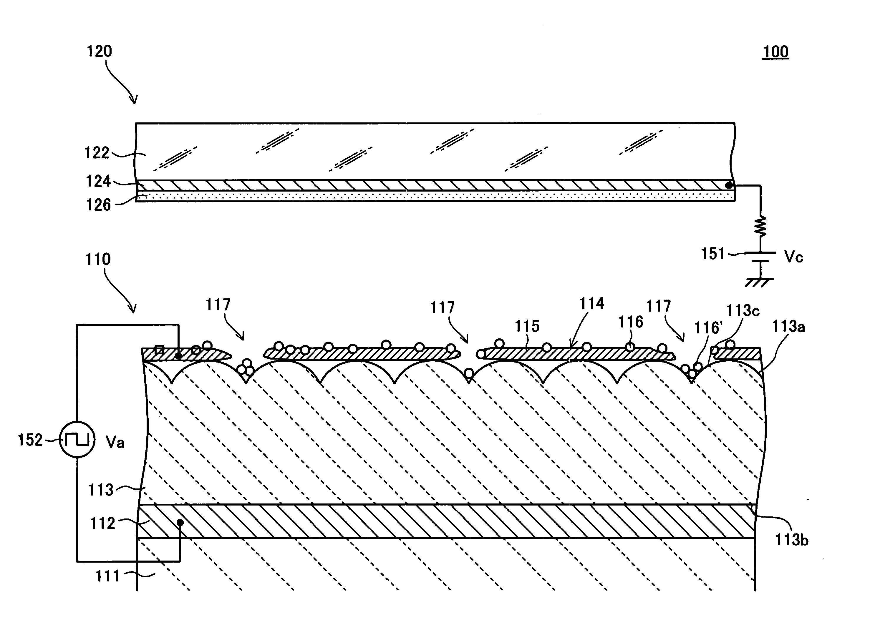
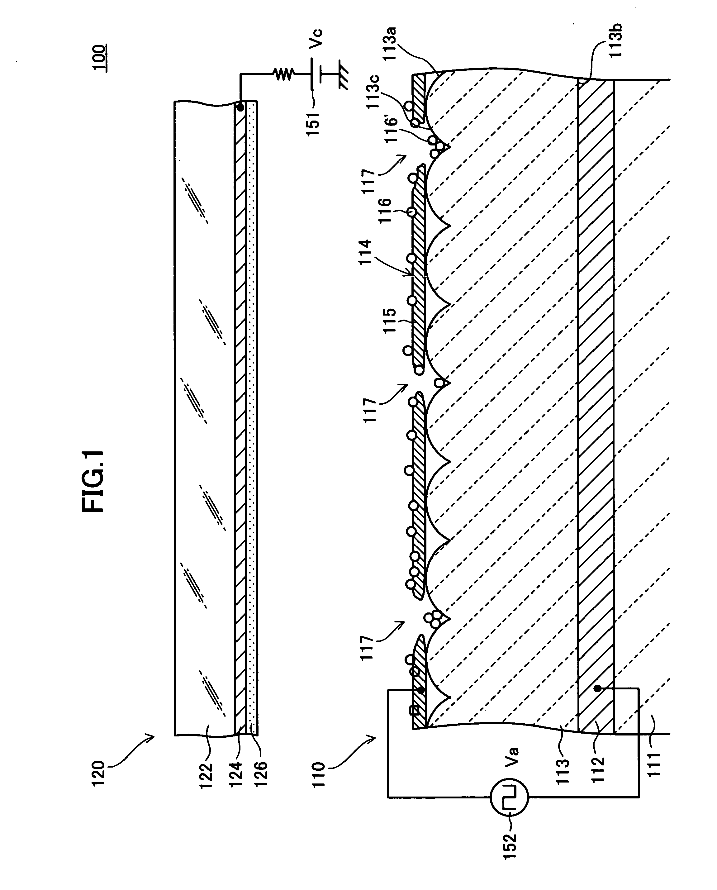
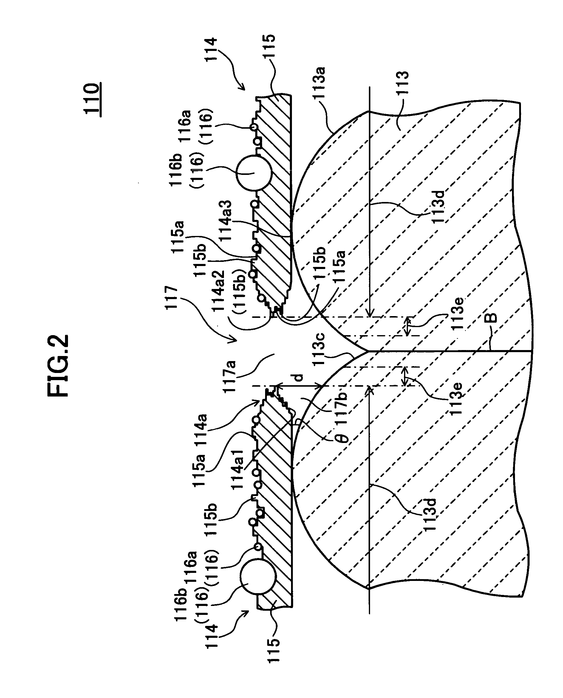
[0175] A specific example (Example 1) of a method for manufacturing the electron emitter 110 (refer to FIG. 1, etc.) having the structure described above according to this embodiment will be described below.

[0176] (Lower Electrode Formation Step)

[0177] On a substrate 111 composed of zirconium oxide (ZrO2) stabilized by yttrium oxide (Y2O3), a layer of a metal paste containing metallic platinum (Pt) is formed by screen printing with a predetermined size and shape. By heat-treating the metal paste layer at a predetermined temperature in the range from about 1,000° C. to about 1,400° C., a lower electrode 112 composed of metallic platinum (Pt) with a thickness of 3 μm is formed so as to be fixed on and integrated with the substrate 111.

[0178] (Emitter Layer Formation Step)

[0179] First, oxides of lead (Pb), magnesium (Mg), zirconium (Zr), titanium (Ti), nickel (Ni), etc. (e.g., lead monoxide (PbO), trilead tetraoxide (Pb3O4), magnesium oxide (MgO), zirconium oxide (ZrO2), titanium o...

example 2

[0201] Another specific example (Example 2) of a method for manufacturing the electron emitter 110 (refer to FIG. 1, etc.) according to this embodiment will be described below.

[0202] In this example, the same ethyl cellulose (thermal decomposition initiation temperature Ts=300° C.; thermal decomposition peak temperature T1=380° C.) as that in Comparative Example described above is used, but the heat treatment step is divided into two stages, i.e., first heat treatment step and second heat treatment step.

example 2-1

[0203] In the first heat treatment step, the temperature is raised to 300° C. over 15 minutes and kept at 300° C. for 5 hours. Subsequently, in the second heat treatment step, the temperature is kept at 400° C. for 2 hours, and then the workpiece is slow-cooled over 15 minutes in the oven.


PUM


Abstract

An electron emitter includes an emitter layer composed of a dielectric material, a first electrode disposed onto a first surface of the emitter layer, and a second electrode disposed onto the first surface, inside, or onto a second surface opposite to the first surface of the emitter layer. A microscopic recess is disposed on a surface of the first electrode. Alternatively, an opening is disposed in the first electrode, the opening exposing the first surface of the emitter layer to the outside of the electron emitter, and a plurality of microscopic protrusions are disposed along the thickness direction of the first electrode at an inner edge of the opening.

Description

BACKGROUND OF THE INVENTION [0001] 1. Field of the Invention [0002] The present invention relates to an electron emitter which can emit electrons when a predetermined electric field is applied. Furthermore, the invention relates to a method for manufacturing the electron emitter. [0003] 2. Description of the Related Art [0004] In an electron emitter of such a type, when a predetermined electric field is applied to an emitter section in a vacuum atmosphere with a predetermined vacuum level, electrons are emitted from the emitter section. [0005] Electron emitters are used as electron beam sources in various devices using electron beams. Examples of such devices include displays, in particular, field emission displays (FEDs), electron beam irradiation devices, light source devices, electronic component manufacturing equipment, and electronic circuit components. [0006] When electron emitters are used in an FED, a plurality of electron emitters are two-dimensionally arrayed in the FED. A...

Claims


Application Information

Patent Timeline
Patent Type & Authority Applications(United States)
IPC IPC(8): H01J9/02
CPCB82Y10/00H01J1/312H01J2201/3125H01J9/022H01J31/127H01J1/32
Inventor OHWADA, IWAOOZAWA, SHUICHIYOSHINO, KOICHIYOKOYAMA, SHOHEI
Owner NGK INSULATORS LTD
Why Eureka
Try Eureka