Nonvolatile semiconductor memory device and data writing method

Inactive Publication Date: 2007-03-29
OKI ELECTRIC IND CO LTD
View PDF2 Cites 18 Cited by
  • Summary
  • Abstract
  • Description
  • Claims
  • Application Information

AI Technical Summary

Benefits of technology

[0030] The present invention is provided with cell resistance compensating means that when the values of parasitic resistances from the sources of memory cells of ith and i+1th rows to their corresponding bit lines are different from one another, selectively inserts a resistance corresponding to the difference between the parasitic resistances upon data writing to thereby

Problems solved by technology

If an error exists, then a contact error display is carried out.
However, the following problems occur in the EPROM of FIG. 2 where the data writing is made thereto in such a procedure as shown in FIG. 4.
Hence, there is a fear that the threshold voltages of the post-writing memory cells are different from each other in terms of the odd-numbered and even-numbered rows, thus causing an error upon reading.
The semiconductor memory device is equipped with a circuit for preventing that cell currents vary due to the fact that diffused resistances or the like take values different between memory cells, thereby degrading reading accuracy, in some cases, causing a m

Method used


Image

  • Nonvolatile semiconductor memory device and data writing method
  • Nonvolatile semiconductor memory device and data writing method
  • Nonvolatile semiconductor memory device and data writing method

Examples


first preferred embodiment

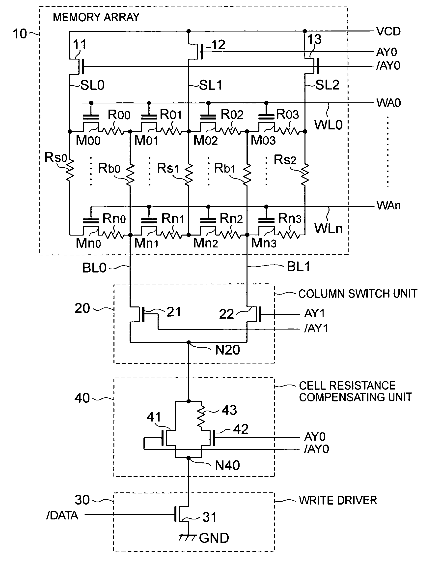
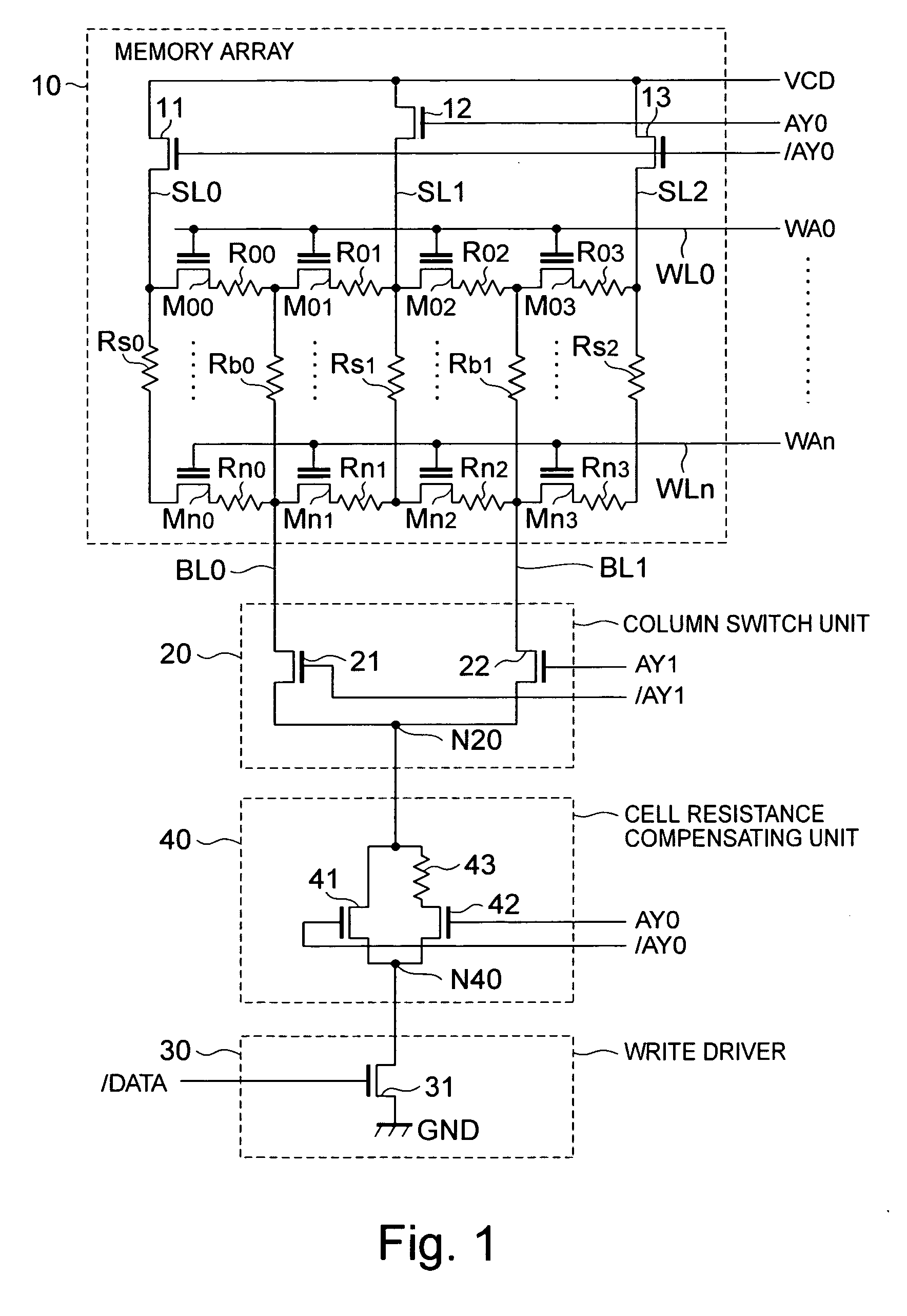
[0043]FIG. 1 is a configurational diagram of an EPROM showing a first embodiment of the present invention. Constituent elements common to those shown in FIG. 2 are given common reference numerals respectively.

[0044] The EPROM includes a cell resistance compensating unit 40 provided between a column switch unit 20 and a write driver 30 in addition to a memory array 10, the column switch unit 20 and the write driver 30 similar to those shown in FIG. 2.

[0045] The memory array 10 is one of such a type that MOS transistors having floating gates for storing electric charges are used as memory cells and the memory cells are arranged in matrix form. The memory array 10 includes selector lines SL0, SL1 and SL2 disposed in parallel, and bit lines BL0 and BL1 disposed in parallel between these selector lines SL0 and SL2. Further, the memory array 10 has a plurality of word lines WLi (where i=0 to n) disposed so as to be orthogonal to the selector lines SL0 through SL2 and the bit lines BL0 a...

second preferred embodiment

[0059]FIG. 6 is a configurational diagram of an EPROM showing a second embodiment of the present invention. Constituent elements common to the constituent elements shown in FIG. 1 are given common reference numerals respectively.

[0060] The EPROM includes a bit line resistance compensating unit 50 provided between a cell resistance compensating unit 40 and a write driver 30 in addition to two sets of memory arrays 100 and 101, a column switch unit 20, the drive driver 30 and the cell resistance compensating unit 40.

[0061] Each of the memory arrays 100 and 101 has a configuration similar to the memory array 10 shown in FIG. 1. The memory arrays 100 and 101 share bit line BL0 and BL1 and have individual or discrete selector lines SL0, SL1 and SL2. These memory arrays 100 and 101 are respectively exclusively selected by select signals AB0 and AB1 supplied to word lines WL0 through WLn.

[0062] The bit line resistance compensating unit 50 is one of such a type that when a memory array (...

third preferred embodiment

[0068]FIG. 7 is a configurational diagram of an EPROM showing a third embodiment of the present invention. Constituent elements common to the constituent elements shown in FIG. 6 are given common reference numerals respectively.

[0069] The EPROM includes a bit line resistance compensating unit 50A provided between a cell resistance compensating unit 40 and a write driver 30 in addition to two sets of memory arrays 100 and 101, a redundant memory array 10R, a column switch unit 20, the drive driver 30 and the cell resistance compensating unit 40.

[0070] Any of the memory arrays 100 and 101 and the redundant memory array 10R has a configuration similar to the memory array 10 shown in FIG. 1. They share bit line BL0 and BL1 and have individual or discrete selector lines SL0, SL1 and SL2. Incidentally, the redundant memory array 10R is disposed between the memory arrays 100 and 101. When either one of the memory arrays 100 and 101 is defective, the redundant memory array 10R is selected...


PUM


Abstract

The present invention aims to eliminate variations in threshold voltage subsequent to the writing of data in an EPROM. When a parasitic resistance between the source of a memory cell (M00) of an even-numbered row and its corresponding bit line (BL0) is larger by a resistance (R00) than a parasitic resistance between the source of a memory cell (M01) of an odd-numbered row and its corresponding bit line (BL0), a cell resistance compensating unit (40) having a compensating resistor (43) whose resistance value is equal to the resistance (R00) is provided between the bit line (BL0) and a ground potential (GND). When the memory cell (M00) is selected by a drain cell power-supply switching address (/AY0), a transistor (41) is turned on by the same signal (/AY0). When the memory cell (M01) is selected by a drain cell power-supply switching address (AY0), a transistor (42) is turned on by the same signal (AY0). The resistor (43) is inserted for the transistor (42), and resistance values from the sources of the memory cells (M00, M01) to the ground potential (GND) become equal to each other. Thus, variations in threshold voltage subsequent to the writing of data can be suppressed.

Description

BACKGROUND OF THE INVENTION [0001] The present invention relates to a nonvolatile semiconductor memory device (hereinafter called “EPROM”) capable of electrically writing data, and particularly to an improvement in data writing accuracy thereof and a data writing method thereof. [0002]FIG. 2 is a schematic configurational diagram of a conventional or prior art EPROM. [0003] The EPROM is equipped with a memory array 10, a column switch unit 20 and a write driver 30. [0004] The memory array 10 is one of such a type that MOS transistors having floating gates for storing electric charges are used as memory cells and the memory cells are arranged in matrix form. The memory array 10 has selector lines SL0, SL1 and SL2 disposed in parallel, and bit lines BL0 and BL1 disposed in parallel between these selector lines SL0 and SL2. Further, the memory array 10 has a plurality of word lines WLi (where i=0 to n) disposed so as to be orthogonal to the selector lines SL0 through SL2 and the bit li...

Claims


Application Information

Patent Timeline
IPC IPC(8): G11C7/10
CPCG11C16/24G11C16/10
Inventor TAKENAKA, TETSURO
Owner OKI ELECTRIC IND CO LTD
Why Eureka
Try Eureka