
Refresh control circuit and method for multi-bank structure DRAM

a control circuit and multi-bank structure technology, applied in the direction of digital storage, instruments, constructions, etc., can solve the problems of increasing power consumption, dram consumption lots, and reducing the charge quantity stored in the capacitor, so as to reduce power consumption

Active Publication Date: 2007-03-29
SK HYNIX INC
View PDF7 Cites 6 Cited by
  • Summary
  • Abstract
  • Description
  • Claims
  • Application Information

AI Technical Summary

Benefits of technology

This approach reduces power consumption by increasing the bank-to-bank refresh interval in proportion to the number of banks refreshed simultaneously, thereby minimizing overall power usage during the refresh operation.

Problems solved by technology

However, charge quantity stored in the capacitor reduces as time passes.
Generally, the DRAM consumes lots of power and requires a predetermined refresh time to perform the refresh operation.
As a matter of course, a power consumption is more increased when the banks are refreshed group by group.

Method used


Image

  • Refresh control circuit and method for multi-bank structure DRAM
  • Refresh control circuit and method for multi-bank structure DRAM
  • Refresh control circuit and method for multi-bank structure DRAM

Examples


first embodiment

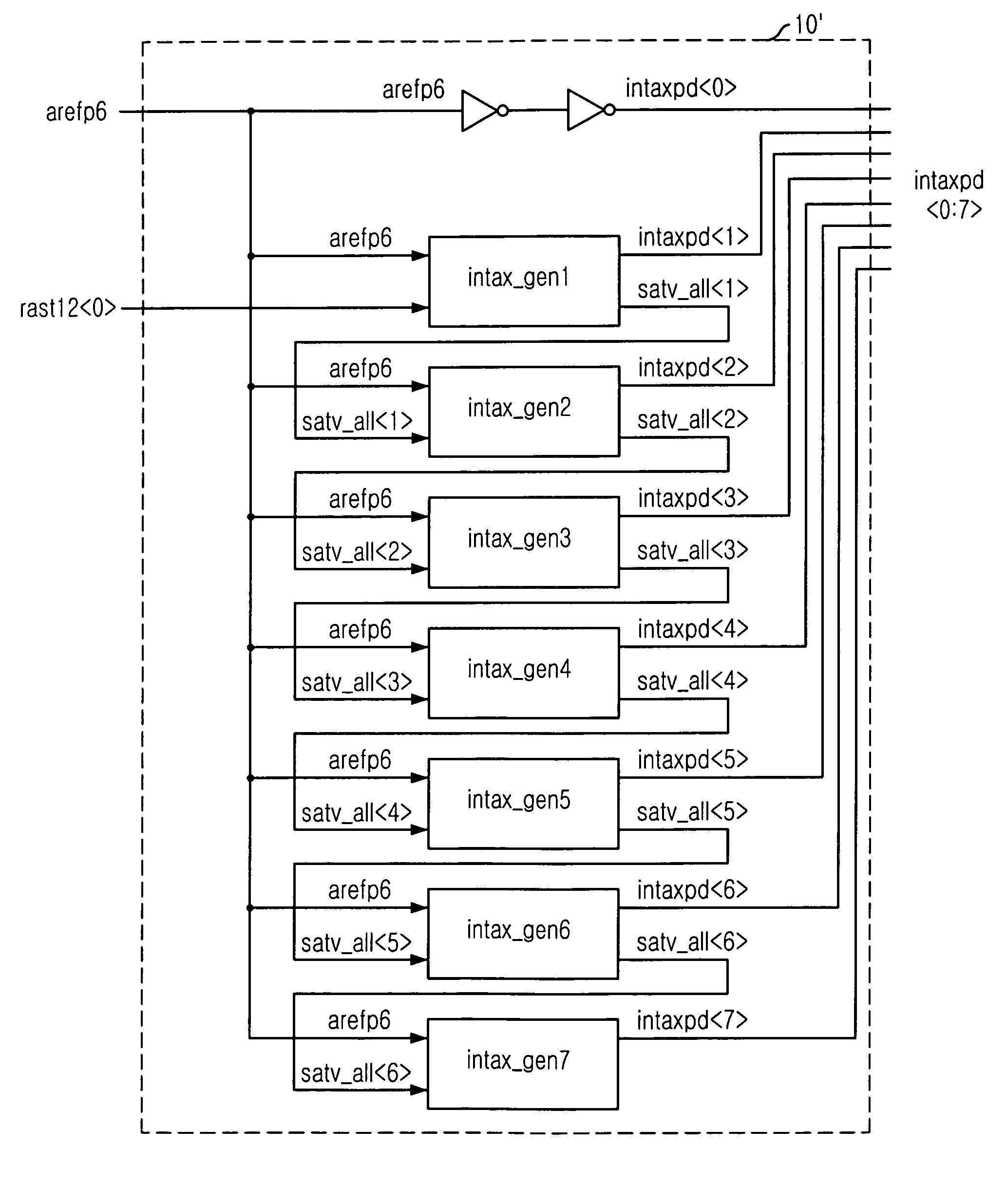
[0043]FIG. 3 is a block diagram showing the bank number signal generator 10′ in accordance with the present invention.

[0044] As shown, the bank number signal generator 10′ includes a plurality of inverters for delaying the refresh signal arefp6 to generate the bank number signal intaxpd0>; and a plurality of internal bank number signal generators, i.e., a first internal bank number signal generator intax_gen1 to a seventh internal bank number signal generator intax_gen7, for generating the bank number signal intaxpd1:7> based on the refresh signal arefp6 and a reference signal rast120>.

[0045] The first internal bank number signal generator intax_gen1 receives the reference signal rast120> for activating a first delay reference signal satv_all1> and the bank number signal intaxpd1> after the predetermined delay time ΔT. The first delay reference signal satv_all1> is used as an enable signal of the second internal bank number signal generator intax_gen2. Then, after the predetermined...

second embodiment

[0047]FIG. 4 is another block diagram showing the bank number signal generator 10′ in accordance with the present invention.

[0048] As shown, the bank number signal generator 10′ includes a plurality of inverters for delaying the refresh signal arefp6 to generate the bank number signal intaxpd0>; and a plurality of internal bank number signal generators, i.e., a first internal bank number signal generator intax_gen1 to a seventh internal bank number signal generator intax_gen7, for generating the bank number signal intaxpd1:7> based on the refresh signal arefp6 and the bank number signal intaxpd0>.

[0049] In comparison with the bank number signal generator 10′ shown in FIG. 3, the bank number signal generator 10′ shown in FIG. 4 uses the bank number signal intaxpd0> as an enable signal of the first internal bank number signal generator intax_gen1 instead of the reference signal rast120> for more simplifying an electric wiring. Since the bank number signal generator 10′ shown in FIG. ...


PUM


Abstract

A refresh control circuit for use in a semiconductor memory device having a plurality of banks, including: a bank number signal generator for generating a plurality of bank number signals having a predetermined delay time between generation timings of the plurality of bank number signals based on a refresh signal and a reference signal; and a bank selection unit for generating a plurality of bank selection signals in response to the plurality of bank number signals and a piled-refresh control signals to thereby refresh the plurality of banks.

Description

FIELD OF INVENTION [0001] The present invention relates to a refresh control circuit capable of controlling a refresh operation of each bank included in a semiconductor memory device and a method thereof. DESCRIPTION OF PRIOR ART [0002] Generally, a semiconductor memory device can be classified into two different types: one is a dynamic random access memory (DRAM) and the other is a static random access memory (SRAM). [0003] Since a memory cell included in the SRAM is formed by four latched transistors, the SRAM can hold its data without a refresh operation as long as power is supplied to the SRAM. [0004] On the contrary, a memory cell included in the DRAM is formed by a transistor and a capacitor; and the capacitor is charged or discharged for the DRAM operation. However, charge quantity stored in the capacitor reduces as time passes. Therefore, the DRAM must be refreshed periodically in order to hold its data contents. Generally, the DRAM consumes lots of power and requires a pred...

Claims


Application Information

Patent Timeline
Patent Type & Authority Applications(United States)
IPC IPC(8): G11C7/00G11C11/406
CPCG11C11/40618G11C11/406E04G5/08E04G5/041E04G5/001
Inventor KWAK, JONG-TAEKANG, SHIN-DEOK
Owner SK HYNIX INC
Features
  • Generate Ideas
  • Intellectual Property
  • Life Sciences
  • Materials
  • Tech Scout
  • Unparalleled Data Quality
  • Higher Quality Content
  • 60% Fewer Hallucinations
Learn More