Strained-induced mobility enhancement nano-device structure and integrated process architecture for CMOS technologies

Inactive Publication Date: 2007-03-29
SEMICON MFG INT (SHANGHAI) CORP
View PDF68 Cites 95 Cited by
  • Summary
  • Abstract
  • Description
  • Claims
  • Application Information

AI Technical Summary

Benefits of technology

[0011] Many benefits are achieved by way of the present invention over conventional techniques. For example, the present technique provides an easy to use process that relies upon conventional technology. In some embodiments, the method provides higher device yields in dies per wafer. Additionally, the method provides a process that is compatible with conventional process technology without substantial modifications to conventional equipment

Problems solved by technology

An integrated circuit or chip fabrication facility can cost hundreds of millions, or even billions, of U.S. dollars.
Making devices smaller is very challenging, as each process used in integrated fabrication has a limit.
Additionally, as devices require faster and faster designs, process limitations exist with certain conventional processes and materials.
Although there have been significant improvements, such devices still

Method used


Image

  • Strained-induced mobility enhancement nano-device structure and integrated process architecture for CMOS technologies
  • Strained-induced mobility enhancement nano-device structure and integrated process architecture for CMOS technologies
  • Strained-induced mobility enhancement nano-device structure and integrated process architecture for CMOS technologies

Examples


Embodiment Construction

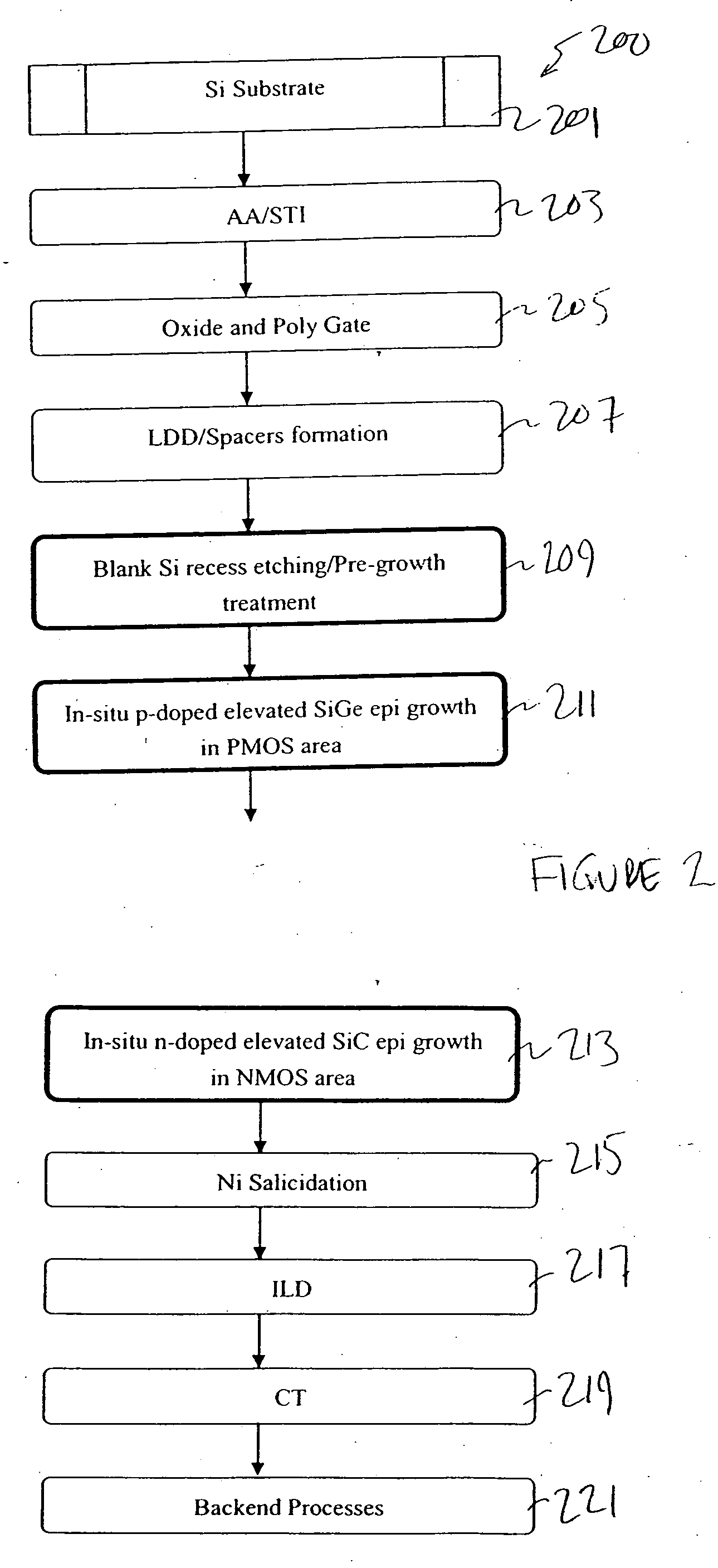
[0019] According to the present invention, techniques for processing integrated circuits for the manufacture of semiconductor devices are provided. More particularly, the invention provides a method and structures for manufacturing MOS devices using strained silicon structures for CMOS advanced integrated circuit devices. But it would be recognized that the invention has a much broader range of applicability.

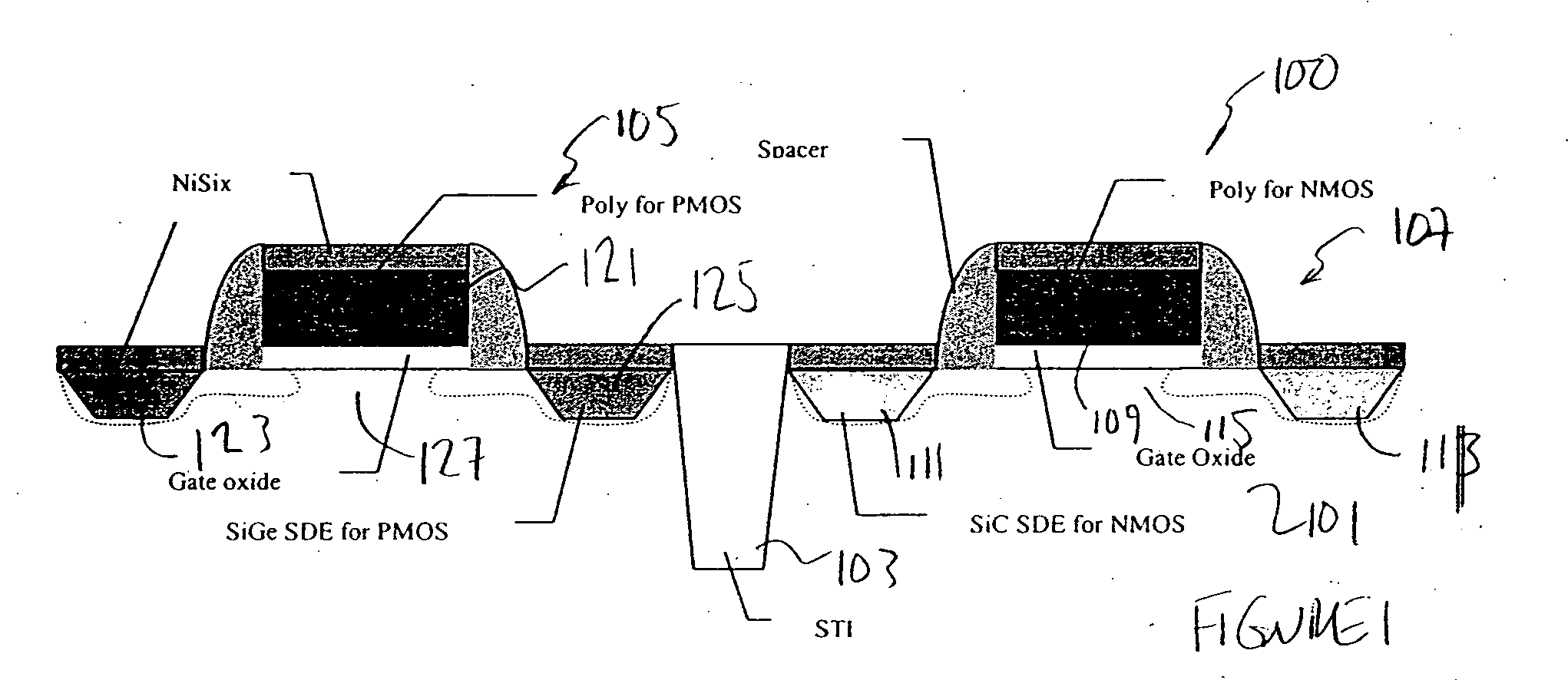
[0020]FIG. 1 is a simplified cross-sectional view diagram of a CMOS device 100 according to an embodiment of the present invention. This diagram is merely an example, which should not unduly limit the scope of the claims herein. One of ordinary skill in the art would recognize many variations, alternatives, and modifications. As shown, the CMOS device includes an NMOS device 107 comprising a gate region 109, a source region 111, a drain region 113 and an NMOS channel region 115 formed between the source region and drain region. Preferably, the channel region has width of less t...


PUM


Abstract

A CMOS semiconductor integrated circuit device. The CMOS device includes an NMOS device comprising a gate region, a source region, and a drain region and an NMOS channel region formed between the source region and drain region. A silicon carbide material is formed within the source region and formed within the drain region. The silicon carbide material causes the channel region to be in a tensile mode. The CMOS device also has a PMOS device comprising a gate region, a source region, and a drain region. The PMOS device has a PMOS channel region formed between the source region and the drain region. A silicon germanium material is formed within the source region and formed with in the drain region. The silicon germanium material causes the channel region to be in a compressive mode.

Description

BACKGROUND OF THE INVENTION [0001] The present invention is directed to integrated circuits and their processing for the manufacture of semiconductor devices. More particularly, the invention provides a method and structures for manufacturing MOS devices using strained silicon structures for advanced CMOS integrated circuit devices. But it would be recognized that the invention has a much broader range of applicability. [0002] Integrated circuits have evolved from a handful of interconnected devices fabricated on a single chip of silicon to millions of devices. Conventional integrated circuits provide performance and complexity far beyond what was originally imagined. In order to achieve improvements in complexity and circuit density (i.e., the number of devices capable of being packed onto a given chip area), the size of the smallest device feature, also known as the device “geometry”, has become smaller with each generation of integrated circuits. [0003] Increasing circuit density...

Claims


Application Information

Patent Timeline
IPC IPC(8): H01L21/8234H01L21/336H01L29/788
CPCH01L21/823807H01L21/823814H01L29/165H01L21/77H01L29/66636H01L29/7843H01L29/7848H01L29/66628
Inventor CHEN, JOHNYANG, SIMON
Owner SEMICON MFG INT (SHANGHAI) CORP
Why Eureka
Try Eureka