Two-dimensional photonic crystal surface-emitting laser
a photonic crystal surface and laser technology, applied in semiconductor lasers, instruments, electrographic processes, etc., can solve the problems of difficult to achieve both merits, and inability to use this laser for a device which requires uniform polarization, and achieve high q-value
- Summary
- Abstract
- Description
- Claims
- Application Information
AI Technical Summary
Benefits of technology
Problems solved by technology
Method used
Image

Examples
Embodiment Construction
[0064] Preferred embodiments of a two-dimensional photonic crystal surface-emitting laser according to the present invention are hereinafter described with reference to the accompanying drawings.
Triangular Lattice Points
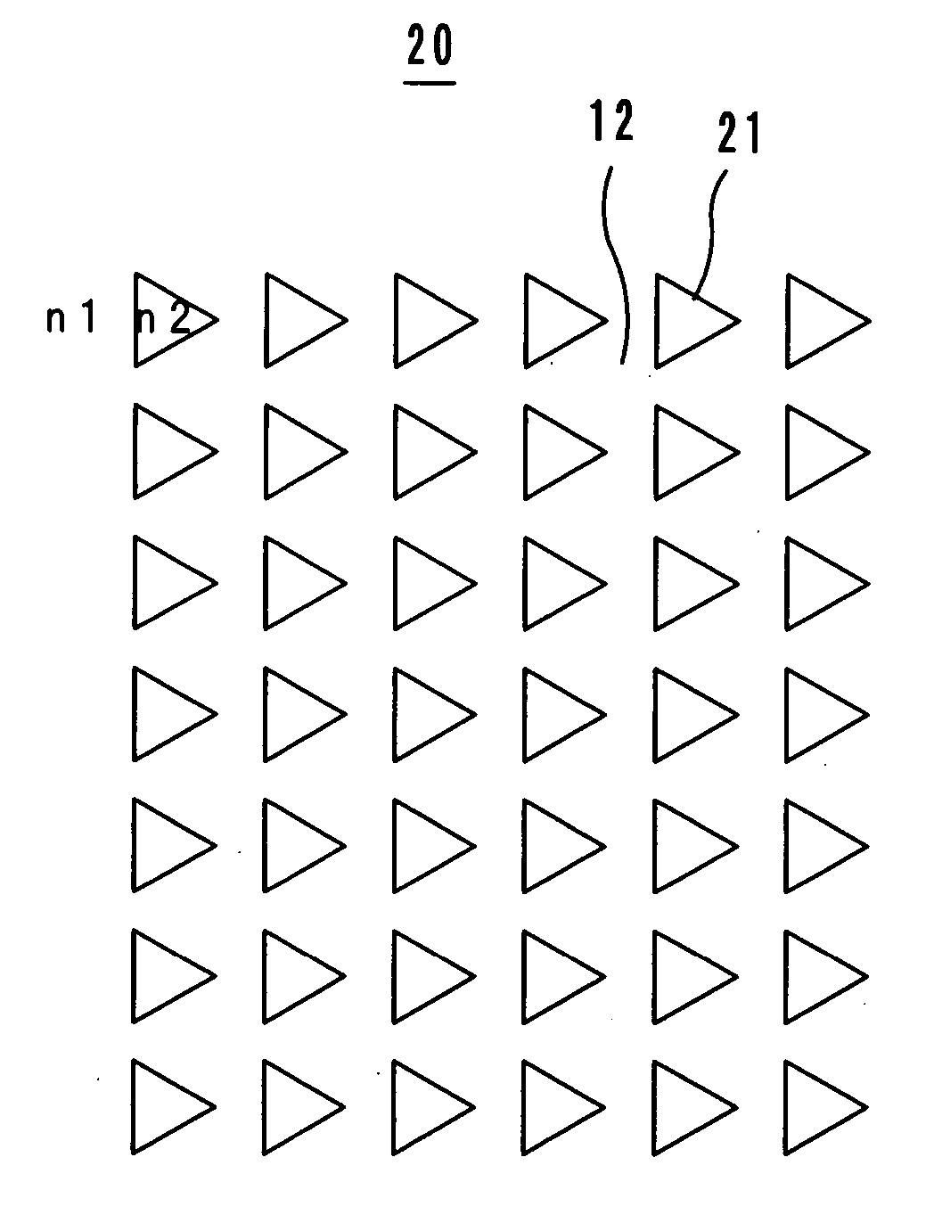
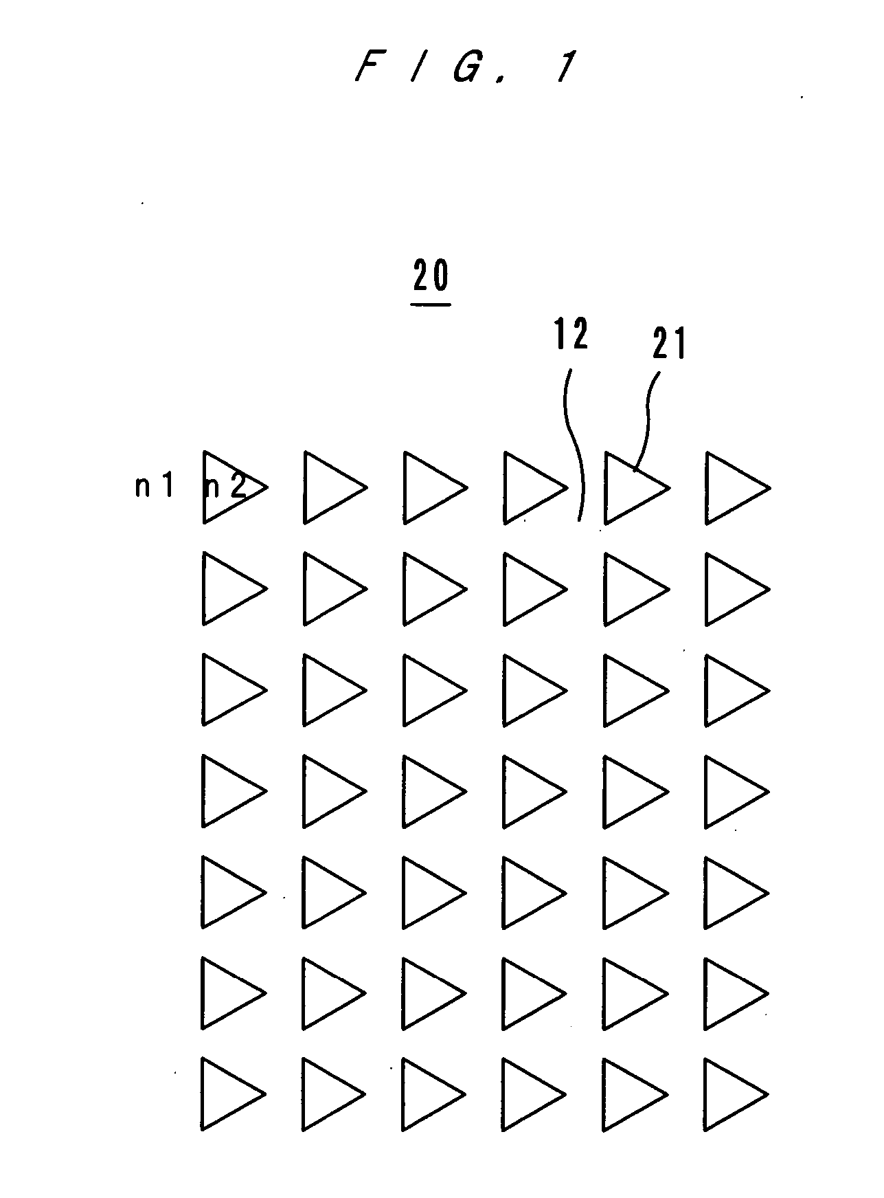
[0065] A two-dimensional photonic crystal surface-emitting laser according to the present invention, of which surface is shown by FIG. 1, is a two-dimensional photonic crystal 20, wherein in a first medium (a lower clad layer) 12 with a refractive index n1, points of a second medium 21 are arranged in a square lattice, so that a photonic crystal periodic structure composed of lattice points is formed. This fundamental structure of the two-dimensional photonic crystal surface-emitting laser according to the present invention is same as that of the conventional surface-emitting laser shown by FIG. 25, and the two-dimensional photonic crystal surface-emitting laser according to the present invention performs surface emission under the principle shown by FIG. 26.
[006...
PUM
 Abstract
Description
Claims
Application Information