Interposer and electronic device fabrication method

a technology of electronic devices and fabrication methods, applied in the direction of fixed capacitor details, stacked capacitors, fixed capacitors, etc., can solve the problems of large inductance due to wiring, insufficient suppression of source voltage variation, and insufficient removal of radio frequency noise, so as to improve the electric characteristics, simplify the test steps, and improve the effect of electric characteristics

Inactive Publication Date: 2007-04-05
FUJITSU LTD
View PDF5 Cites 46 Cited by
  • Summary
  • Abstract
  • Description
  • Claims
  • Application Information

AI Technical Summary

Benefits of technology

[0018] An object of the present invention is to provide an interposer which allows the test steps to be simplified, and an electronic device fabrication method using the interposer.
[0021] According to the present invention, the respective upper electrodes of a plurality of thin-film capacitors are electrically interconnected by an interconnection, a plurality of through-electrodes are electrically connected to the upper electrodes of the plural thin-film capacitors by the interconnection, and the plural through-electrodes are electrically interconnected by the interconnection, whereby the probe of a test system is connected to one of the plural through-electrodes to thereby test the plural thin-film capacitors at once. According to the present invention, the plural thin-film capacitors can be tested at once without the necessity of connecting the probe sequentially to the respective through-electrodes of the plural thin-film capacitors. The test steps can be simplified.
[0022] According to the present invention, the undersurface the upper surface and the side surfaces of each thin-film capacitor are covered by the barrier film for prohibiting the diffusion of hydrogen or water, whereby the capacitor dielectric film of the thin-film capacitors are prevented from being reduced by hydrogen or water emitted from the resin layers, etc. Thus, the present invention can provide an interposer including thin-film capacitors of good electric characteristics.
[0023] According to the present invention, the conductor plugs are connected to the upper electrodes via the conductive barrier film, and through-electrodes are connected to the lower electrodes via the conductive barrier film, whereby in fabricating the interposer and using the interposer, hydrogen or water are prohibited from arriving at the upper electrodes and the lower electrodes via the conductor plugs and the through-electrodes by the conductive barrier films. Thus, the present invention can provide an interposer which can surely prevent the capacitor dielectric film of the thin-film capacitors from being reduced by hydrogen or water and includes thin-film capacitors of better electric characteristics.
[0024] According to the present invention, the base of the interposer is formed of the resin layers alone and does not use a semiconductor substrate as the base. It is not necessary to form the through-holes in the semiconductor substrate, etc., which are difficult to pass through-holes. Thus, according to the present invention, the fabrication cost of the interposer can be decreased.
[0025] According to the present invention, the interposer using the resin layers alone as the base is formed on the substrate, the substrate is removed with the interposer adhered by the supporting substrate, and the supporting substrate is removed after the interposer has been mounted on the substrate, whereby even when the base are formed of the resin layers alone, the deformation of the interposer can be prevented. Furthermore, according to the present invention, the interposer is adhered by means of the heat foaming type double-sided tape, and when the interposer does not have to be supported by the supporting substrate any more, the interposer can be removed easily from the supporting substrate. Thus, the present invention can fabricate a highly reliable electronic device at low cost.

Problems solved by technology

However, when decoupling capacitors are mounted near an LSI mounted on a circuit board, the LSI and the decoupling capacitors are electrically connected to the decoupling capacitors via interconnection formed in the circuit board, and large inductance due to the wiring is present.
Due to the large inductance between the LSI and the decoupling capacitors, the source voltage variation cannot be sufficiently suppressed, and the radio-frequency noises cannot be sufficiently removed.
Accordingly, it is difficult to test the proposed interposer in a short period of time and at low costs.

Method used


Image

  • Interposer and electronic device fabrication method
  • Interposer and electronic device fabrication method
  • Interposer and electronic device fabrication method

Examples


Embodiment Construction

One Embodiment

[0044] The interposer according to a first embodiment of the present invention and the method for fabricating the interposer, and a method for fabricating an electronic device using the interposer will be explained with reference to FIGS. 1 to 18.

[0045] (Interposer and Electronic Device)

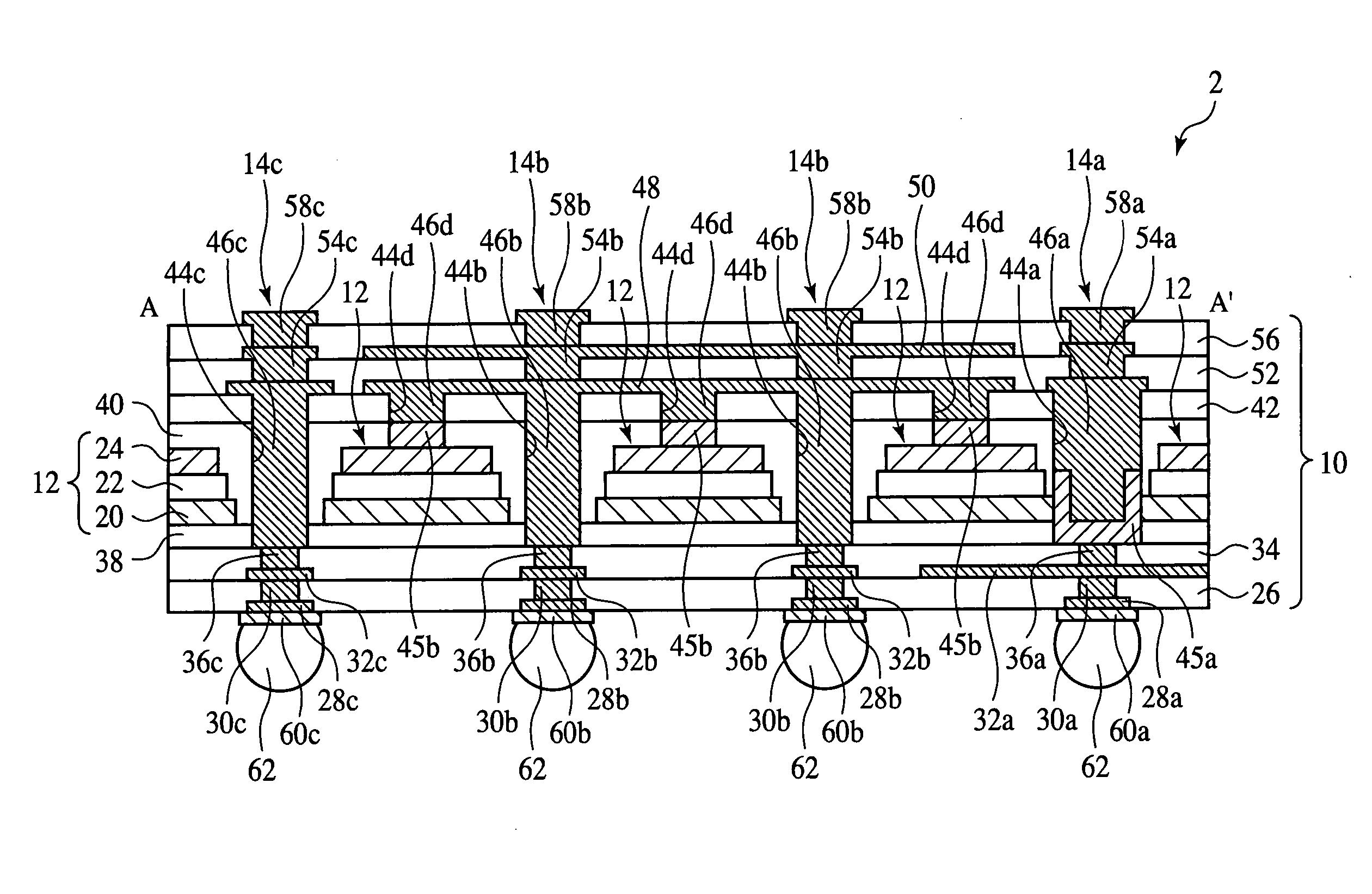
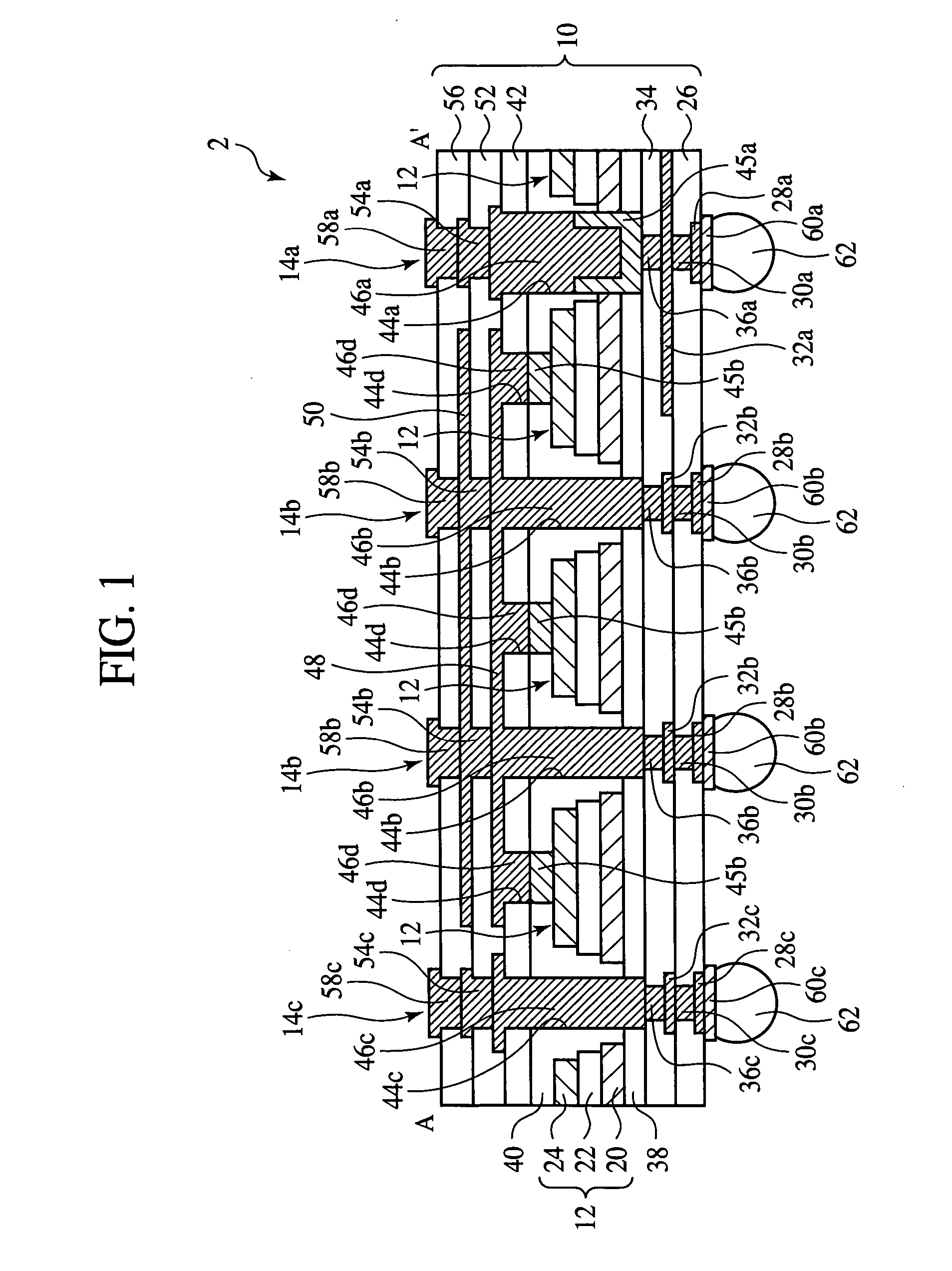
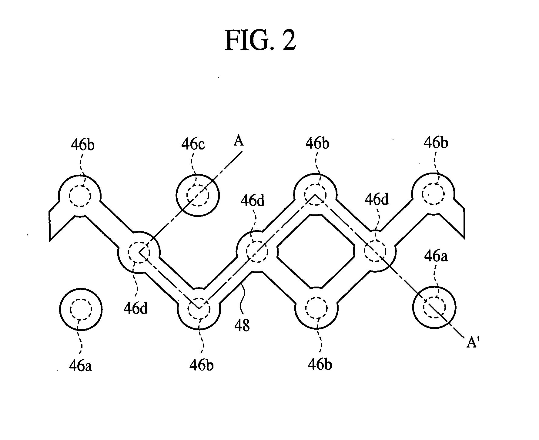
[0046] First, the interposer and the electronic device according to the present embodiment will be explained with reference to FIG. 1. FIG. 1 is a sectional view of the interposer according to the present embodiment (Part 1). FIG. 2 is a plane view of a part of the interposer according to the present embodiment. FIG. 3 is a sectional view of the interposer according to the present embodiment (Part 2). FIG. 4 is a sectional view of the electronic device according to the present embodiment.

[0047] As illustrated in FIG. 1, the interposer according to the present embodiment comprises a base 10 of a plurality of resin layers laid one on the other, a plurality of thin-film capacitors 12 b...


PUM

PropertyMeasurementUnit
heat resistance temperatureaaaaaaaaaa
thicknessaaaaaaaaaa
densityaaaaaaaaaa

Abstract

An interposer 2 comprising a base 10 formed of a plurality of resin layers 26, 34, 42, 52, 56; a thin-film capacitor 12 buried in the base 10, including a lower electrode 20, a capacitor dielectric film 22 and an upper electrode 24; a first through-electrode 14b formed through the base 10 and electrically connected to the upper electrode 24 of the thin-film capacitor 12; and a second through-electrode 14a formed through the base 10 and electrically connected to the lower electrode 20 of the thin-film capacitor 12, further comprising: an interconnection 48 buried in the base 10 and electrically connected to the respective upper electrodes 24 of a plurality of the thin-film capacitors 12, a plurality of the first through-electrodes 14b being electrically connected to the upper electrodes 24 of said plurality of the thin-film capacitors 12 via the interconnection 48, and said plurality of the first through-electrodes 14b being electrically interconnected by the interconnections 48.

Description

CROSS-REFERENCE TO RELATED APPLICATION [0001] This application is based upon and claims priority of Japanese Patent Application No. 2005-287065, filed on Sep. 30, 2005, the contents being incorporated herein by reference. BACKGROUND OF THE INVENTION [0002] The present invention relates to an interposer, and an electronic device fabrication method using the interposer, more specifically, an interposer which can simplify test steps, and an electronic device fabrication method using the interposer. [0003] Recently, in digital LSIs (Large Scale Integrated circuits), etc., typically microprocessors, the operation speed increase and the power consumption decrease have been made. [0004] To stably operate an LSI in a GHz band-radio-frequency region and at low voltage, it is very important to suppress the source voltage variation due to abrupt changes of the load impedance, etc. of the LSI and to remove radio-frequency noises of the power source. [0005] Conventionally, the source voltage cha...

Claims


Application Information

Patent Timeline
Patent Type & Authority Applications(United States)
IPC IPC(8): H01G4/236
CPCH01G4/232Y10T29/49165H01L21/6835H01L2221/68345H01L2224/16H01L2924/01046H01L2924/01077H01L2924/01078H01L2924/01079H01L2924/19041H01L2924/30105H01L2924/3011H05K1/112H05K1/141H05K1/162H05K3/007H05K3/4602H05K2201/0179H05K2201/09509H05K2201/096H05K2201/10378H05K2201/10674H05K2203/016H05K2203/0191Y10T29/49128Y10T29/49155Y10T29/49126Y10T29/4913Y10T29/49153H01G4/30H01L2224/05568H01L2224/05573H01L2224/16235H01L2224/16265H01L2924/00014H01L2924/15311H01L2224/05599
Inventor SHIOGA, TAKESHIISHIZUKI, YOSHIKATSUBANIECKI, JOHN DAVIDKURIHARA, KAZUAKI
Owner FUJITSU LTD
Why Eureka
Try Eureka