Unlock instant, AI-driven research and patent intelligence for your innovation.

Precision position determining method

a technology of precision position and determination method, which is applied in the direction of distance measurement, mechanical measurement arrangement, instruments, etc., can solve the problems of high-cost techniques that require stringent environmental conditions, complicated lithographic methods, and complicated procedures, and achieve the same positional precision

Inactive Publication Date: 2007-04-05
PANASONIC CORP
View PDF7 Cites 5 Cited by
  • Summary
  • Abstract
  • Description
  • Claims
  • Application Information

AI Technical Summary

Benefits of technology

[0017] The present invention is embodied in a method for locating a point on a surface of a microstructure with a precision and stability approachi

Problems solved by technology

The feature sizes used to form photonic crystals and the precise alignment requirements of these features complicate manufacture of these materials.
One challenge in producing micro-circuitry is preventing shorts between components and nano-wires which are located ever closer together.
These high-cost techniques usually require stringent environmental conditions, such as high vacuum or clean room condition.
All the lithographic methods require a series of complicated procedures, which involve generating multiple masks and using photoresist.
Still forming submicron features with a laser beam smaller the wavelength of the laser is a difficult issue.
Currently, no technique is known to be able to achieve better than 10-nm positioning precision on a performed substrate nondestructively.
Although other techniques such as a UV optical stepper can achieve such precision on a blank substrate, those techniques cannot be applied to a preformed structure due to lacking precision surface topology feedback.
The charged beam apparatus can achieve very good precision but it intends to be destructive.

Method used


Image

  • Precision position determining method
  • Precision position determining method
  • Precision position determining method

Examples


Embodiment Construction

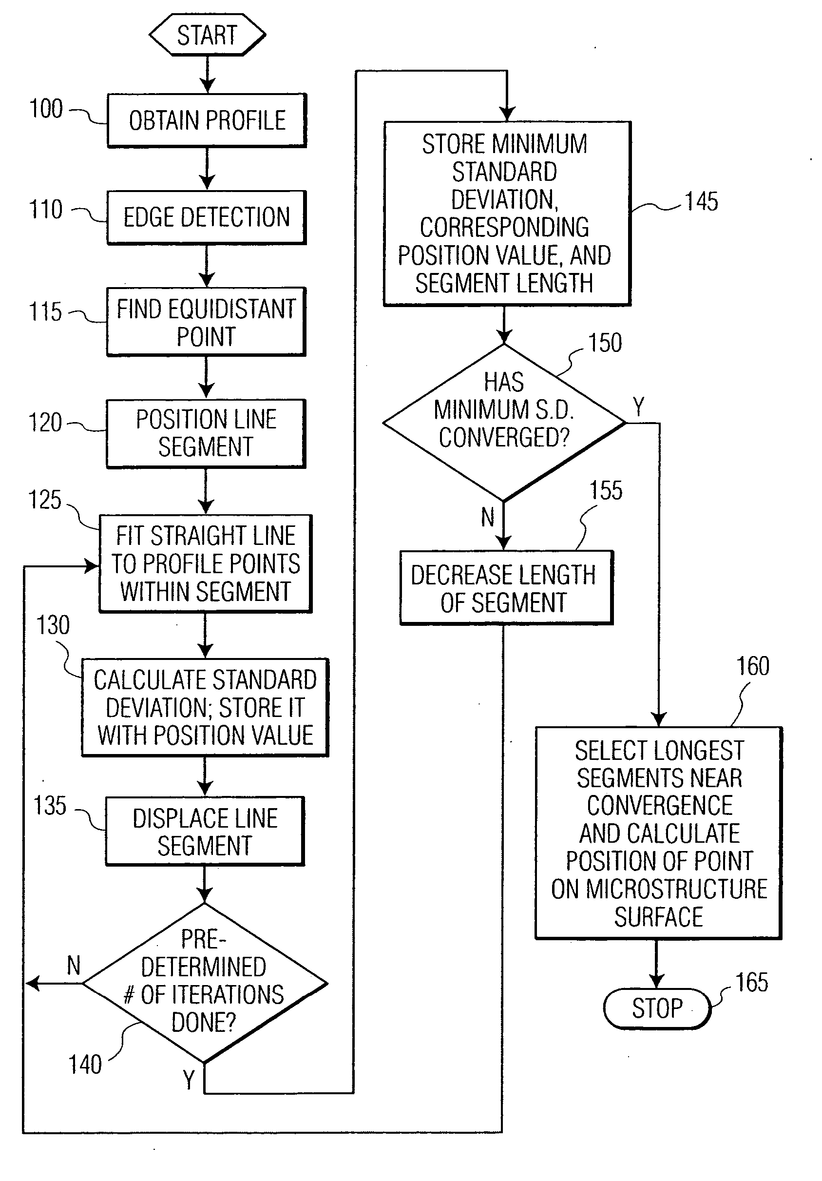
[0028]FIG. 1 illustrates an embodiment of a method for locating a point on a surface of a microstructure with a positioning accuracy and stability potentially less than 10 nm. The term microstructure is to be understood as a physical structure having at least one feature smaller than 1 micrometer.

[0029] To start, a profile of the microstructure is measured 100 to obtain respective positions of at least two edges of the microstructure surface. The profile is comprised of position points, designating lateral positions on the surface, and profile points, giving the height or depth of the surface at each position point. One profile point is associated with each position point. The profile may be obtained by any method with sufficiently small spatial resolution, such as an atomic force microscope (AFM), a near-field scanning optical microscope (NSOM), an NSOM probe operating as an AFM probe, a scanning tunneling microscope (STM), an interferometer, a white light interferometer, a stereo...


PUM

PropertyMeasurementUnit
Nanoscale particle sizeaaaaaaaaaa
Sizeaaaaaaaaaa
Microstructureaaaaaaaaaa

Abstract

A method for generating a surface profile of a microstructure. The profile is processed to determine positions of at least two edges and an approximate center point of the profiled surface. Segments of points on the determined profile are fit to a straight line centered at the approximate center point. A standard deviation of the fitted points is measured. The length and position of the segment are varied until a minimum standard deviation is determined and the process is repeated for segments having different lengths. The point is determined from the longest segment having a standard deviation approximately equal to the minimum standard deviation of all of the segment lengths.

Description

FIELD OF THE INVENTION [0001] The present invention concerns a method for laser machining of submicron features on microstructures, including nanostructures. This method may also allow mass manufacturing, customization or repair of generic electronic and mechanical microstructures. More specifically it concerns the precision position locking of a micromachining tool. BACKGROUND OF THE INVENTION [0002] As products get smaller and smaller, there is increased demand for micro-electrical-mechanical systems (MEMS), micro-optical devices and photonic crystals. With this demand, there is an associated increased interest in micro- and nano-machining. Numerous applications exist for MEMS. As a breakthrough technology, allowing unparalleled synergy between previously unrelated fields such as biology and microelectronics, new MEMS applications are emerging at a rapid pace, expanding beyond those currently identified or known. Additional applications in quantum electric devices, micro-optical d...

Claims


Application Information

Patent Timeline
IPC IPC(8): G06F15/00B81C99/00G01Q30/04G01Q60/10G01Q60/18G01Q60/24
CPCB23K26/04B81C1/00626B81C2201/0143
Inventor CHENG, CHEN-HSIUNG
Owner PANASONIC CORP