Flip-flop circuit

a flip-flop circuit and circuit technology, applied in the field of flip-flop circuits, can solve the problems of large loading, unnecessarily large loading, and the signal path using the clocks clk and clkb is required to pass through the transmission gate tb>, and achieve the effect of high impedance state and achieve the stability

Active Publication Date: 2007-04-12
SK HYNIX INC
View PDF13 Cites 3 Cited by
  • Summary
  • Abstract
  • Description
  • Claims
  • Application Information

AI Technical Summary

Benefits of technology

[0011] It is, therefore, a primary object of the present invention to provide a flip-flop circuit capable of achieving its stability in a high impedance state by using a feedback inverter of a latch.

Problems solved by technology

In this case, however, a signal path using the clocks CLK and CLKB is required to pass through the transmission gates T1 and T2 unnecessarily.
In particular, if the size of a driver at the last stage is large, the size of each of the transmission gates T1 and T2 becomes large, thus causing large loading due to increase of junction capacitance.
In such case, since a signal must pass through a total of one transmission gate and two-stage inverters IV2 and IV3 to transmit input data, there may be a time delay for the signal transmission during a high-frequency operation.
Thus the conventional bypass flip-flop circuit is limited in terms of operating frequency.

Method used


Image

  • Flip-flop circuit
  • Flip-flop circuit
  • Flip-flop circuit

Examples


Embodiment Construction

[0018] Hereinafter, a flip-flop circuit in accordance with the present invention will be described in detail with reference to the accompanying drawings.

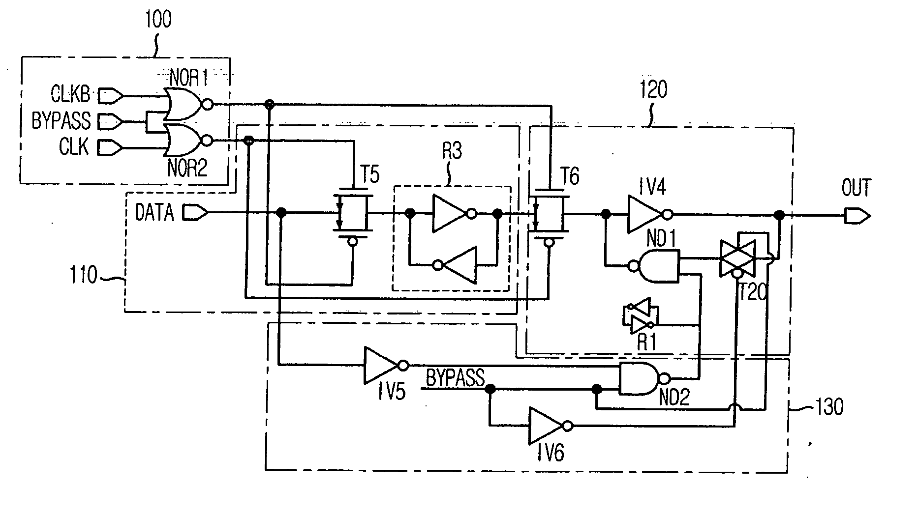
[0019]FIG. 2 is a circuit diagram of a bypass flip-flop circuit in accordance with an embodiment of the present invention.

[0020] The bypass flip-flop circuit of the present invention includes an input controller 100, a latch portion 110, an output controller 120 and a latch controller 130.

[0021] As shown in FIG. 2, the input controller 100 is provided with NOR gates NOR1 and NOR2 for logically operating clocks CLK and CLKB and a bypass signal BYPASS, respectively. The NOR gate NOR1 NOR-operates the clock CLKB and the bypass signal BYPASS, and the NOR gate NOR2 NOR-operates the clock CLK and the bypass signal BYPASS.

[0022] The latch portion 110 is composed of a transmission gate T5 and a latch R3. The transmission gate T5 selectively allows an output of data DATA depending on outputs of the NOR gates NOR1 and NOR2. Applied to an ...


PUM


Abstract

Signal delivery delay margin of a bypass flip-flop circuit is stabilized during high-frequency operation. An input controller for logically operating a bypass signal and a clock produces first and second output signals having different states depending on whether or not the bypass signal is activated. A latch circuit latches input data based on the first and second output signals. A latch controller logically operates the bypass signal and input data to generate a third output signal having a different state depending on whether or not the bypass signal is activated. An output controller is switched in response to the states of the first and second output signals for logically combining an output signal selected from the latch circuit and the third output signal to provide the output signal.

Description

FIELD OF THE INVENTION [0001] The present invention relates to a flip-flop circuit; and, more particularly, to a technology capable of achieving a stable signal delivery during a high-frequency operation by improving a signal delivery delay margin of a bypass flip-flop circuit. DESCRIPTION OF RELATED ART [0002] Latches and flip-flops generally have been used as storage devices for storing data in digital circuits. Among those devices, the flip-flops are utilized for sequential devices that sample inputs thereto and modify their outputs at a time determined by a clock signal. In contrast, the latches are used as sequential devices that continuously observe all inputs thereto and alter their outputs at any time regardless of the clock signal. [0003]FIGS. 1A and 1B are circuit diagrams of conventional bypass flip-flops. [0004] Each of the conventional flip-flop circuits includes first and second latch portions 10 and 20, and a bypass portion 30. [0005] The first latch portion 10 is pro...

Claims


Application Information

Patent Timeline
Patent Type & Authority Applications(United States)
IPC IPC(8): H03K19/173
CPCH03K3/012H03K3/356156
Inventor KIM, KYUNG-HOONKWON, TAE-HEUI
Owner SK HYNIX INC
Why Eureka
Try Eureka