Exposure apparatus, exposure method, and semiconductor device manufacturing method

a technology of exposure apparatus and exposure method, applied in the field of photolithography, can solve the problems of difficult to increase the lithography margin, difficult to further reduce the wavelength of exposure light, and failure to form a fine resist pattern

Inactive Publication Date: 2007-04-12
KK TOSHIBA
View PDF6 Cites 5 Cited by
  • Summary
  • Abstract
  • Description
  • Claims
  • Application Information

AI Technical Summary

Benefits of technology

[0008] According to an aspect of the invention, there is provided an exposure apparatus comprising: an illumination optical system which forms an effective light source having a first polarization area where a mask pattern is illuminated with polarized light dominated by an electric vector component radial from a center position on an effective light source plane, and a second polarization area where the mask pattern is illuminated with light whose electric vector vibration is not biased in a specific direction; and a projection optical system which projects an image of the mask pattern onto an object to be processed.

Problems solved by technology

However, constraints on glass for use and the like make it difficult to further reduce the wavelength of exposure light.
However, it is difficult to increase the lithography margin when forming a fine pattern such as a hole pattern, failing to form a fine resist pattern into a desired shape.

Method used


Image

  • Exposure apparatus, exposure method, and semiconductor device manufacturing method
  • Exposure apparatus, exposure method, and semiconductor device manufacturing method
  • Exposure apparatus, exposure method, and semiconductor device manufacturing method

Examples


first modification

(First Modification)

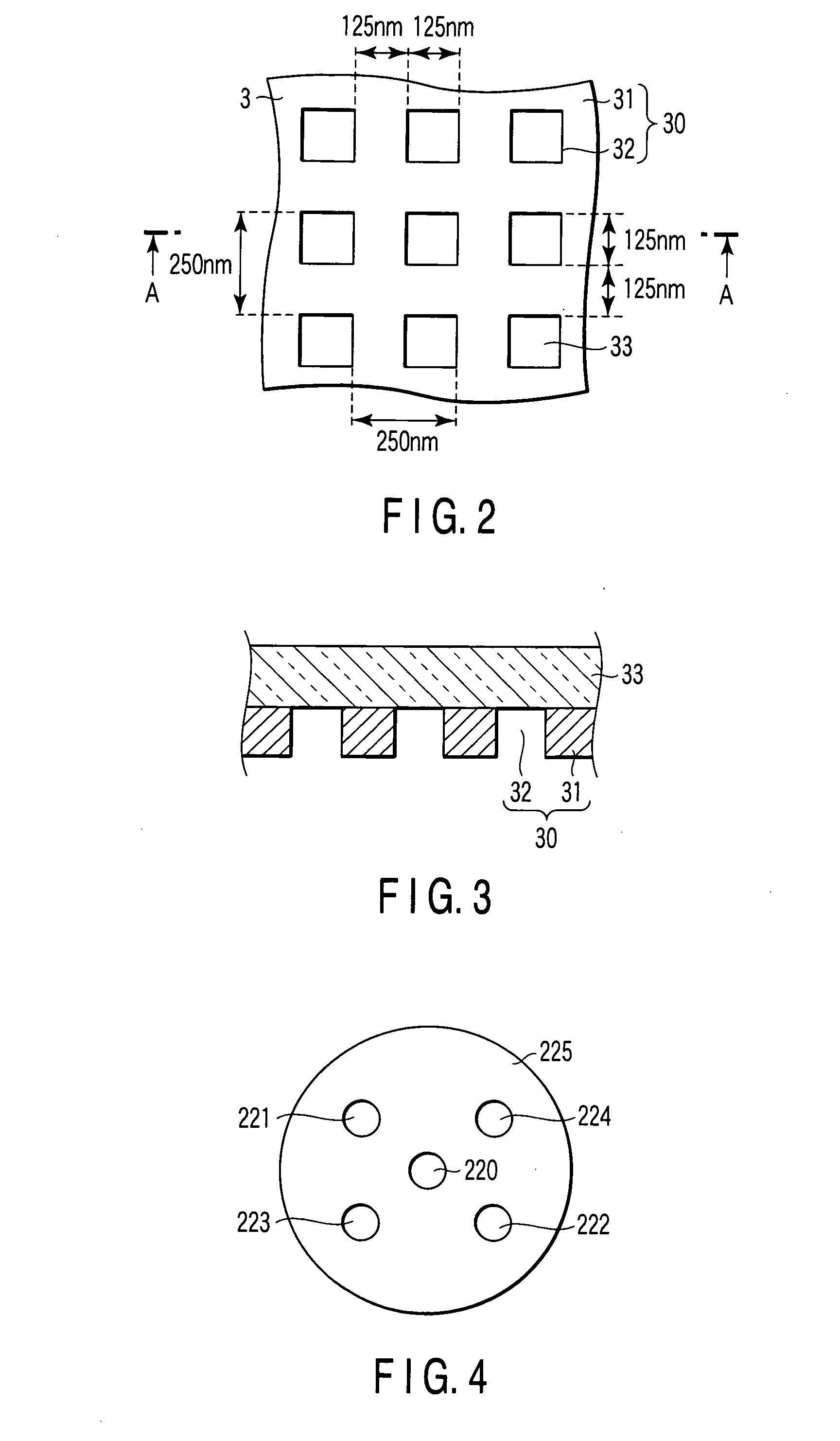
[0076] The first modification to the embodiment of the present invention will explain another illumination shape. The first modification will describe a case of forming a hole pattern at different lengthwise and breadthwise pitches. As shown in FIG. 22, the space widths between adjacent apertures 32 of the mask pattern 30 are 125 nm lengthwise and 225 nm breadthwise. The mask pattern 30 shown in FIG. 22 preferably adopts pentapole illumination as shown in FIG. 23. In the pentapole illumination shown in FIG. 23, the positions of the first to fourth eccentric areas 221 to 224 shift from the axis by 45°. That is, a straight line coupling the first eccentric areas 221 and the second eccentric areas 222 crosses a straight line coupling the third eccentric areas 223 and the fourth eccentric areas 224 so that the angle between the two straight lines are not 90°. The first and second obliquely incident light components from the first to fourth eccentric areas 221 to 224 ...

second modification

(Second Modification)

[0078] In the embodiment of the present invention, the radial polarization area, non-polarization area, or circular polarization area is formed on the effective light source plane 23, as shown in FIG. 6. In the second modification to the embodiment of the present invention, small-σ / unpolarized illumination as shown in FIG. 24 and quadrupole / radially polarized illumination as shown in FIG. 25 may be separately formed. More specifically, the small-σ / unpolarized illumination shown in FIG. 24 forms the center area 220. The quadrupole / radially polarized illumination shown in FIG. 25 form the first to fourth eccentric areas 221 to 224.

[0079] An exposure method according to the second modification to the embodiment of the present invention will be explained with reference to the flowchart of FIG. 26.

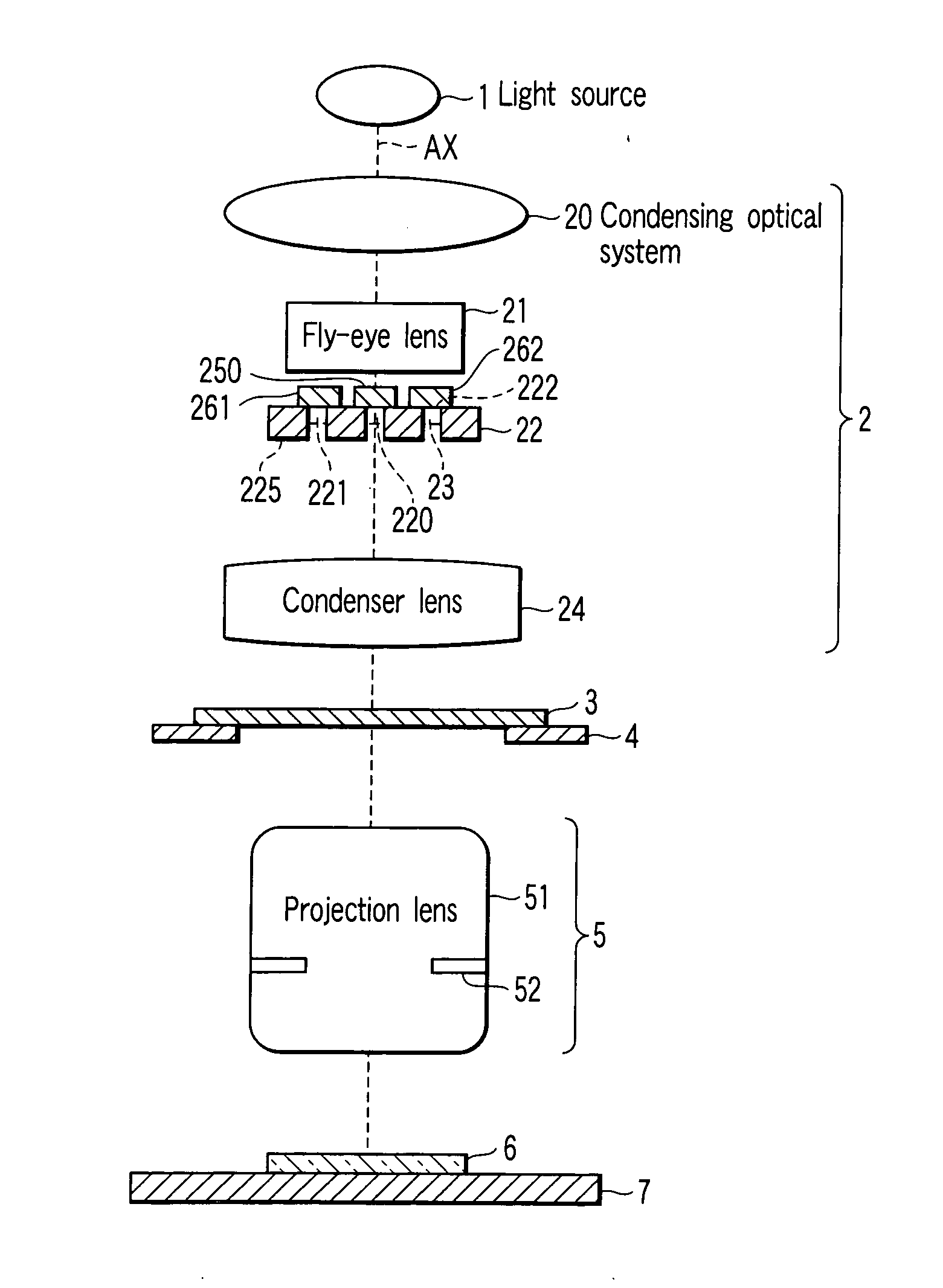
[0080] (1) In step S1, a photomask 3 is set on the mask stage 4, as shown in FIG. 1. In step S2, an object 6 to be processed is set on the wafer stage 7.

[0081] (2) In st...


PUM


Abstract

According to an aspect of the invention, there is provided an exposure apparatus including an illumination optical system which forms an effective light source having a first polarization area where a mask pattern is illuminated with polarized light dominated by an electric vector component radial from a center position on an effective light source plane, and a second polarization area where the mask pattern is illuminated with light whose electric vector vibration is not biased in a specific direction; and a projection optical system which projects an image of the mask pattern onto an object to be processed.

Description

CROSS-REFERENCE TO RELATED APPLICATIONS [0001] This application is based upon and claims the benefit of priority from prior Japanese Patent Application No. 2005-294689, filed Oct. 7, 2005, the entire contents of which are incorporated herein by reference. BACKGROUND OF THE INVENTION [0002] 1. Field of the Invention [0003] The present invention relates to photolithography and, more particularly, to an exposure apparatus and an exposure method used to form a fine pattern in manufacturing a semiconductor device or the like, and to a semiconductor device manufacturing method. [0004] 2. Description of the Related Art [0005] The manufacture of a semiconductor device using photolithography uses a projection exposure apparatus. The projection exposure apparatus irradiates, with illumination light, a mask pattern drawn on a photomask (reticle) and formed from a transmitting portion and light-shielding portion. The projection exposure apparatus projects light having passed through the photoma...

Claims


Application Information

Patent Timeline
Patent Type & Authority Applications(United States)
IPC IPC(8): G03B27/72
CPCG03F7/70091G03F7/70566
Inventor FUKUHARA, KAZUYASATO, TAKASHI
Owner KK TOSHIBA
Why Eureka
Try Eureka