Method for Performing Post-Synthesis Circuit Optimization

a post-synthesis circuit and optimization technology, applied in the field of circuit optimization, can solve the problems of large yield loss in the high-performance bin, low-power devices are vulnerable to process variability, and high-power devices are also vulnerable to process variability

Inactive Publication Date: 2007-04-12
INTELLECTUAL VENTURES HLDG 40
View PDF1 Cites 6 Cited by
  • Summary
  • Abstract
  • Description
  • Claims
  • Application Information

AI Technical Summary

Benefits of technology

[0008] In accordance with a preferred embodiment of the present invention, a gate-level description of a circuit to be optimized is initially provided. The gates within the circuit are electrically characterized. In addition, the semiconductor manufacturing process intended to be utilized to manufacture the circuit is also characterized. Statistical gate delay models for performing optimization are generated by utilizing the electrical characterization information from the gate characterization and the process variability data from the semiconductor manufacturing process characterization. A robust linear program for gate sizing is formulated by utilizing the generated statistical gate delay models. The robust linear program is then transformed to a second order conic program. Finally, the second order conic program is solved to yield an optimal gate size for each gate within the circuit.

Problems solved by technology

Low-power devices are vulnerable to process variability because devices with low Vth tend to exhibit larger sensitivity to variations.
On the other hand, high-power devices are also vulnerable to process variability because they tend to have a very high leakage power, which leads to a larger yield loss in the high-performance bin.
In addition, leakage power (or standby power) of a device increases as the geometry of the device decreases.

Method used


Image

  • Method for Performing Post-Synthesis Circuit Optimization
  • Method for Performing Post-Synthesis Circuit Optimization
  • Method for Performing Post-Synthesis Circuit Optimization

Examples


Embodiment Construction

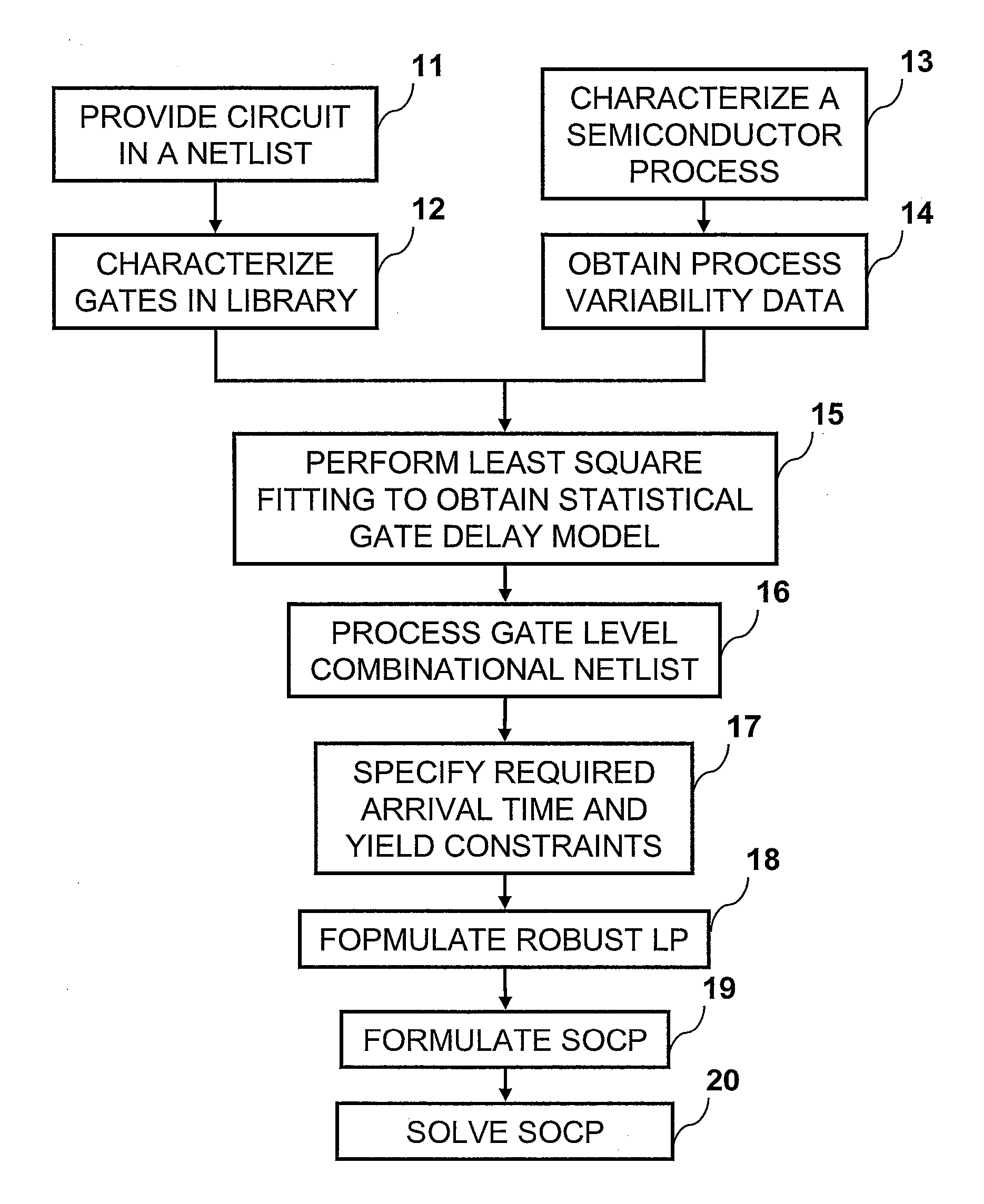
[0014] Referring now to the drawings and in particular to FIG. 1, there is illustrated a high-level logic flow diagram of a method for performing post-synthesis circuit optimization, in accordance with a preferred embodiment of the present invention. Initially, a circuit ready to be optimized is represented in a gate-level description (i.e., a netlist), as shown in block 11. The logic gates within the circuit come from a gate cell library that may include a variety of simple gates, such as NAND2, NAND3, NAND4, NOR2, NOR3, INVERTER, and other complex modules. The size of each gate within the gate cell library determines the speed with which a gate produces a correct output. The gates in the gate 11 cell library are then electrically characterized (or simulated) using a circuit simulator, as depicted in block 12. A circuit simulator, such as HSPICE, can be utilized to characterize the dependence of a gate's delay on the gate's size and the load “seen” by the gate at the gate's output....


PUM


Abstract

Two methods for post-synthesis circuit optimization are disclosed. In both methods, the underlying variability in process parameters is captured through a robust linear program. The robust linear program is then reformulated as a second order conic program that possesses special structural properties to allow for a computationally efficient solution by using interior point optimization methods. The first method treats gate delays as uncertain quantities and obtains the optimal sizes for gates in a circuit under a probabilistically specified circuit timing target. The second method optimizes total circuit power by using a combination of dual threshold voltage assignment and gate sizing. Both circuit power and timing are treated probabilistically.

Description

RELATED APPLICATION [0001] The present application claims priority under 35 U.S.C. §119(e)(1) to provisional application No. 60 / 725,958 filed on Oct. 11, 2005, the contents of which are incorporated herein by reference.BACKGROUND OF THE INVENTION [0002] 1. Technical Field [0003] The present invention relates to circuit optimization in general, and in particular to methods for performing post-synthesis circuit optimization on an integrated circuit design. [0004] 2. Description of Related Art [0005] Generally speaking, an increase in variability of key process parameters, such as effective channel length (Leff) and threshold voltage (Vth), can significantly impact the design and optimization of integrated circuits in the nanometer regime. The increase in variability can be attributed to many factors, such as manufacturing control problems, emergence of new systematic variation-generating mechanisms, etc. But the most important factor that causes an increase in variability is the incre...

Claims


Application Information

Patent Timeline
Patent Type & Authority Applications(United States)
IPC IPC(8): G06F17/50
CPCG06F17/5022G06F30/33
Inventor ORSHANSKY, MICHAELMANI, MURARI
Owner INTELLECTUAL VENTURES HLDG 40
Why Eureka
Try Eureka