Supercharge Your Innovation With Domain-Expert AI Agents!

Semiconductor memory device and electronic apparatus

Inactive Publication Date: 2007-04-19
SHARP KK
View PDF3 Cites 11 Cited by
  • Summary
  • Abstract
  • Description
  • Claims
  • Application Information

AI Technical Summary

Benefits of technology

[0020] As shown above, the semiconductor storage device of the invention is a semiconductor storage device such as flash memory, ferroelectric memory or mask ROM, in which values related cell currents of memory cells, through which a constant current flows in their selected state, are read out by the cell-current related value read circuit, and the values related cell currents and the reference value obtained by the reference value generation section are compared with each other, by which data of the individual memory cells are read out. Accordingly, by determining stored information with the use of the values related to cell currents of memory cells and the reference value, information stored in the memory cells can be decided without using any conventional reference cell. Also, even if the distribution of cell current values is varied among word lines or changed with time, information stored in the memory cells can accurately be read out by virtue of the use of values related to cell currents that represent a characteristic that cell currents and discharge period (or charge period) are generally inversely proportional to each other. Further, since the reference value is obtained by the reference value generation section, the need for the conventional reference cell is eliminated. Moreover, since it is no longer necessary to reset the cell current value of the reference cell in response to changes of current values of memory cells due to disturb or the like, as would be involved in the prior art, circuitry and operation of the semiconductor storage device can be simplified to a large extent, so that the chip area can be cut down. Further, since the reference value generation section determines the reference value in parallel processing during the discharge (or charge) of bit lines, read operation can be carried out without loss of access time.
[0105] Also, with the electronic equipment of the invention, there can be fulfilled electronic equipment of low cost and high reliability by using the semiconductor storage device.

Problems solved by technology

In these semiconductor storage devices, in which cell currents flowing through memory cells are changed to store data, even for memory cells having identical data stored therein, it is difficult to make their individual cell currents fully coincident with one another.
However, since overlaps of cell current distributions among different data would incur a difficulty in correctly deciding data, verify operation is performed together with write operation or erase operation so that those respective distributions are not overlapped with one another.
This causes a problem that even memory cells connecting to one word line differ in distribution state of cell current values from one another, giving rise to positional differences of gap regions that separate the distributions of cell currents according to different data from one another.
However, in this conventional semiconductor storage device, since a plurality of reference cells are provided for each word line, there is a problem that the chip area increases to a large extent.
Further, in this conventional semiconductor storage device, since disturb is influential until the verify operation in writing is performed, there is a difficulty in making a decision as to how long intervals the verify operation should be done at.
Moreover, this semiconductor storage device has a problem that extra time is required to re-set the cell current values of the reference cells.

Method used


Image

  • Semiconductor memory device and electronic apparatus
  • Semiconductor memory device and electronic apparatus
  • Semiconductor memory device and electronic apparatus

Examples


Embodiment Construction

[0138] Hereinbelow, a semiconductor storage device and electronic equipment of the present invention will be described in detail by embodiments thereof illustrated in the accompanying drawings.

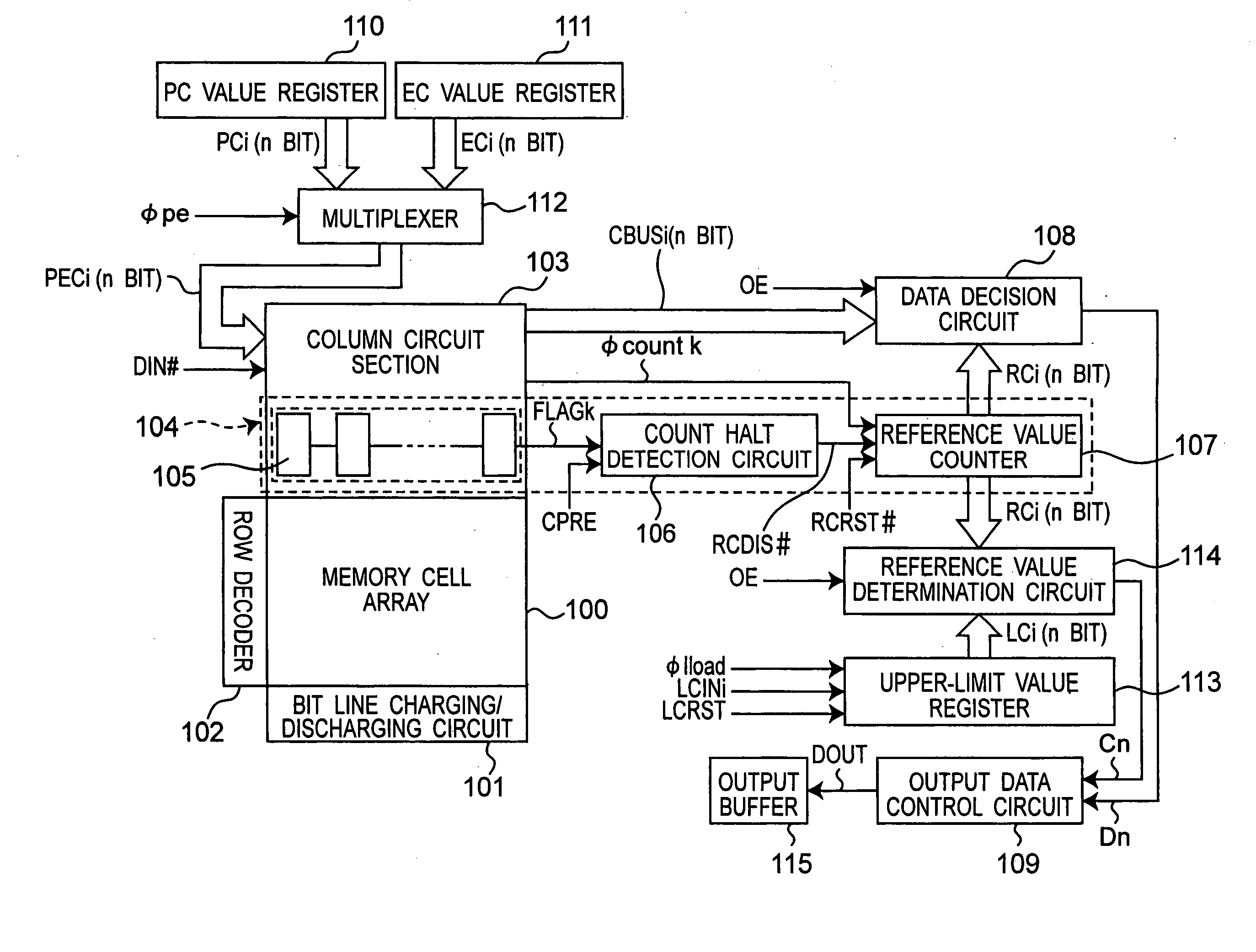
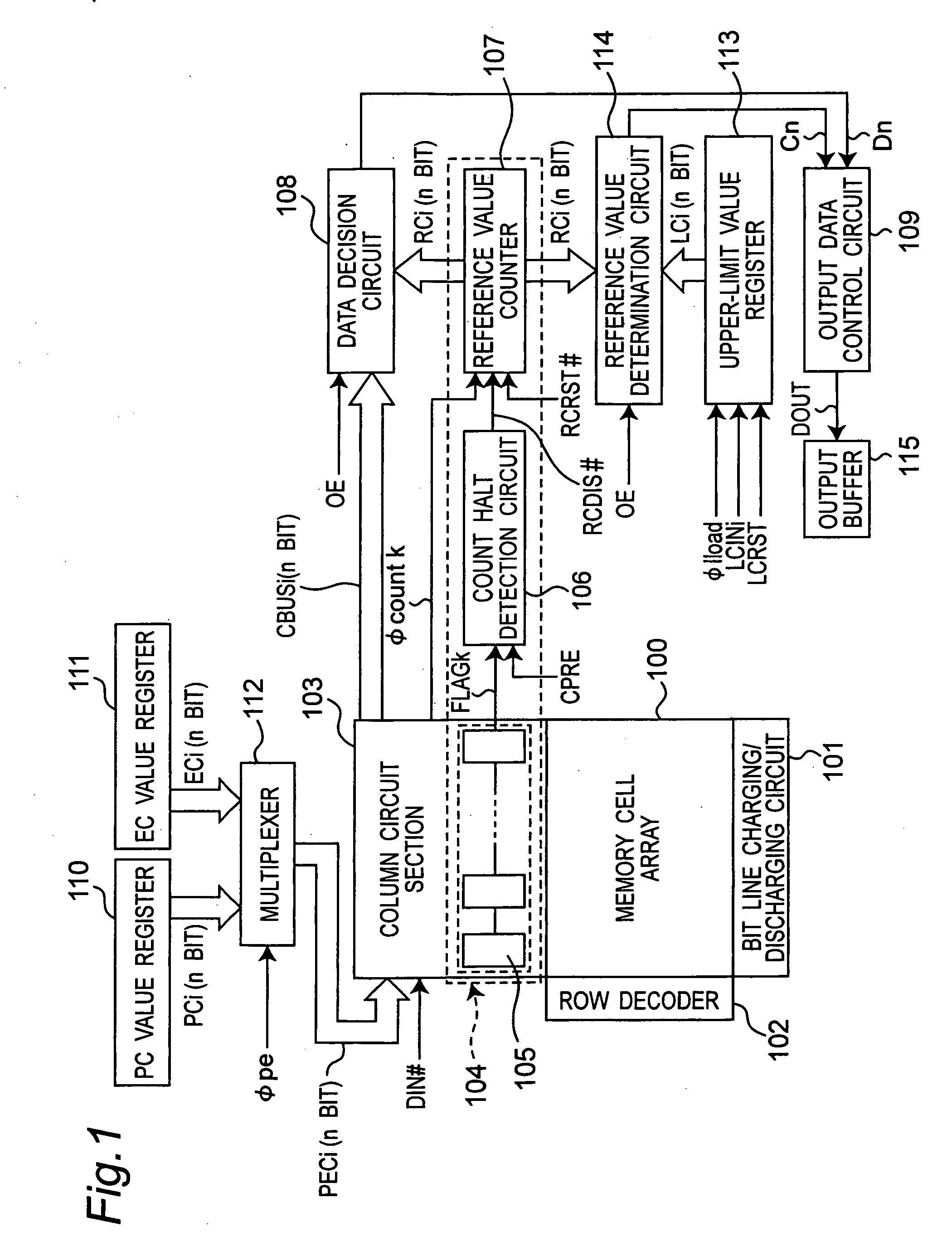
[0139]FIG. 1 shows a block diagram of the whole semiconductor storage device of the embodiment of the invention.

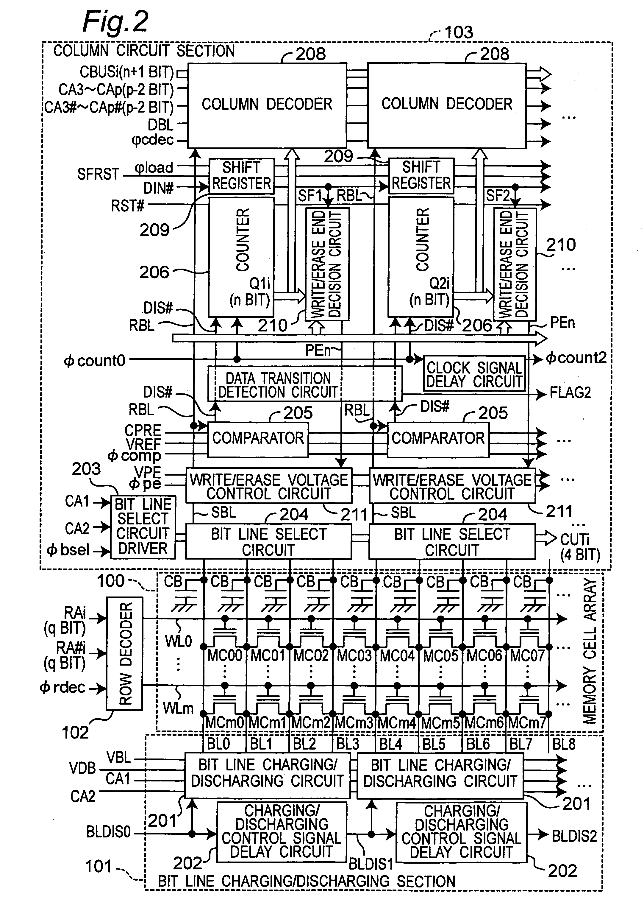
[0140] This semiconductor storage device, as shown in FIG. 1, includes a memory cell array 100 in which a plurality of nonvolatile memory cells (shown in FIG. 2) are arrayed, a row decoder 102 which is an example of a word line select circuit for selecting bit lines (shown in FIG. 2) connected to input / output terminals of a plurality of memory cells of the memory cell array 100, a bit line charging / discharging section 101 for performing charge and discharge for the bit lines, and a column circuit section 103 having a comparator (shown in FIG. 2) for comparing potentials of the bit lines with a reference potential, a counter (shown in FIG. 2) for counting, based on an output signal ...


PUM


Abstract

In the semiconductor storage device, in a read operation, a bit line charging / discharging section 101 performs discharge of bit lines of a memory cell array 100, and a counter counts discharge periods over which the potentials of bit lines come to a specified potential, based on a comparison result of a comparator comparing a potential of a bit line with a reference potential. Based on the comparison result, a reference value generation section 104 generates a reference value (RCi) for determining information stored in each of the memory cells. The above count value (CBUSi) and the above reference value (RCi) are compared with each other by a data decision circuit 108. Based on the comparison result, an output data control circuit 109 outputs information stored in each of the memory cells. This semiconductor storage device suppresses increases in chip area and power consumption and outputs memory cell information accurately.

Description

CROSS-REFERENCE TO RELATED APPLICATIONS [0001] This nonprovisional application claims priority under 35 U.S.C. §119(a) on Patent Application No(s). 2005-290992 filed in Japan on Oct. 4, 2005, the entire contents of which are hereby incorporated by reference.BACKGROUND OF THE INVENTION [0002] The present invention relates to semiconductor storage devices and electronic equipment and, more particularly, to a semiconductor storage device, as well as electronic equipment using the device, which includes nonvolatile memory cells such as flash memory cells or mask ROM (read-only memory) cells. [0003] Recently, nonvolatile memories such as flash memory, ferroelectric memory and mask ROM have been widely used as semiconductor storage devices for use of data storage or code storage in portable telephones and digital cameras. Also, capacity increases for increasing the storage capacity has been going on and on more than ever. [0004] In these semiconductor storage devices, in which cell curren...

Claims


Application Information

Patent Timeline
IPC IPC(8): G11C16/06
CPCG11C16/28
Inventor OHTA, YOSHIJI
Owner SHARP KK
Features
  • R&D
  • Intellectual Property
  • Life Sciences
  • Materials
  • Tech Scout
  • Unparalleled Data Quality
  • Higher Quality Content
  • 60% Fewer Hallucinations
Learn More