Method for manufacturing magnetoresistive element

a technology of magnetoresistive elements and manufacturing methods, which is applied in the direction of magnetic bodies, instruments, superimposed coating processes, etc., can solve the problems of insufficient element characteristics, low purity, and difficulty in satisfying both the ra and mr ratio of ccp-cpp elements fabricated by using the above method

Inactive Publication Date: 2007-04-26
KK TOSHIBA
View PDF4 Cites 21 Cited by
  • Summary
  • Abstract
  • Description
  • Claims
  • Application Information

AI Technical Summary

Benefits of technology

[0014] performing two stages of oxidation treatments in which a partial pressure of an oxidizing gas in a first oxidation treatment is set to 1 / 10 or less of a partial pressure of an oxidizing gas in a second oxidation treatment, two stages of nitriding treatments in which a partial pressure of a nitriding gas in a first nitriding treatment is set to 1 / 10 or less of a partial pressure of a nitriding gas in a second nitriding treatment or two stages of oxynitriding treatments in which a partial pressure of an oxynitriding gas in a first oxynitriding treatment is set to 1 / 10 or less of a partial pressure of an oxynitriding gas in a second oxynitriding treatment, and the second metal layer being irradiated with an ion beam or RF plasma of a rare gas in the first oxidation treatment, the first nitriding treatment or the first oxynitriding treatment.

Problems solved by technology

However, a metal CPP element in which the pinned layer, the spacer layer and the free layer are made of metal exhibits only a low resistance change ΔRA when a current supplied perpendicularly to the film plane, even though a giant magnetoresistance effect is obtained, because the element has a low element resistance.
However, for detection of weak signals from a medium with a high recording density of 200 to 500 Gbpsi, the CCP-CPP element fabricated by using the above method has difficulty in satisfying both the areal resistance RA and the MR ratio.
Studies by the present inventors suggested that insufficient element characteristics are caused by low purity of the current paths in the insulating layer.

Method used


Image

  • Method for manufacturing magnetoresistive element
  • Method for manufacturing magnetoresistive element
  • Method for manufacturing magnetoresistive element

Examples


example 1

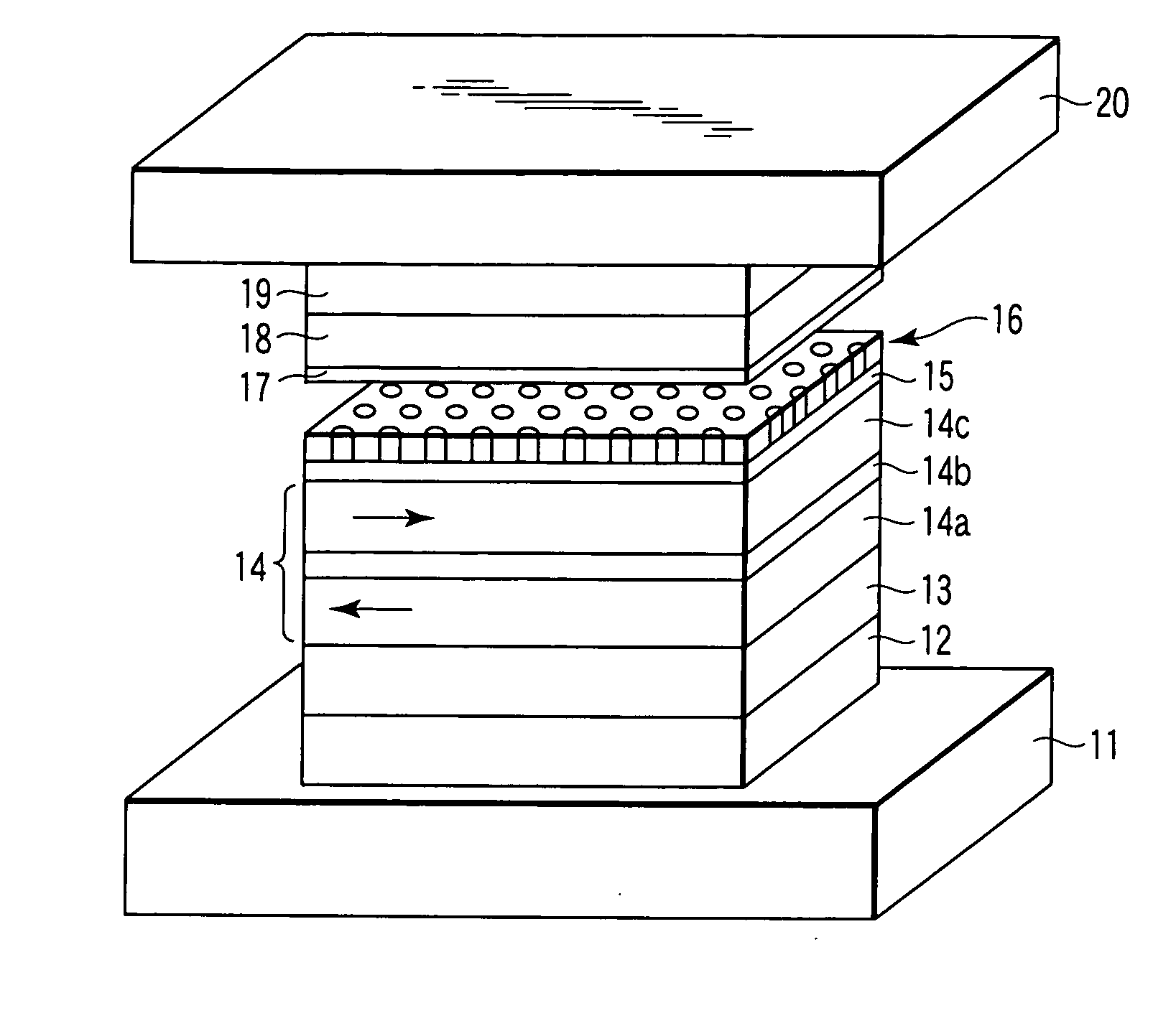
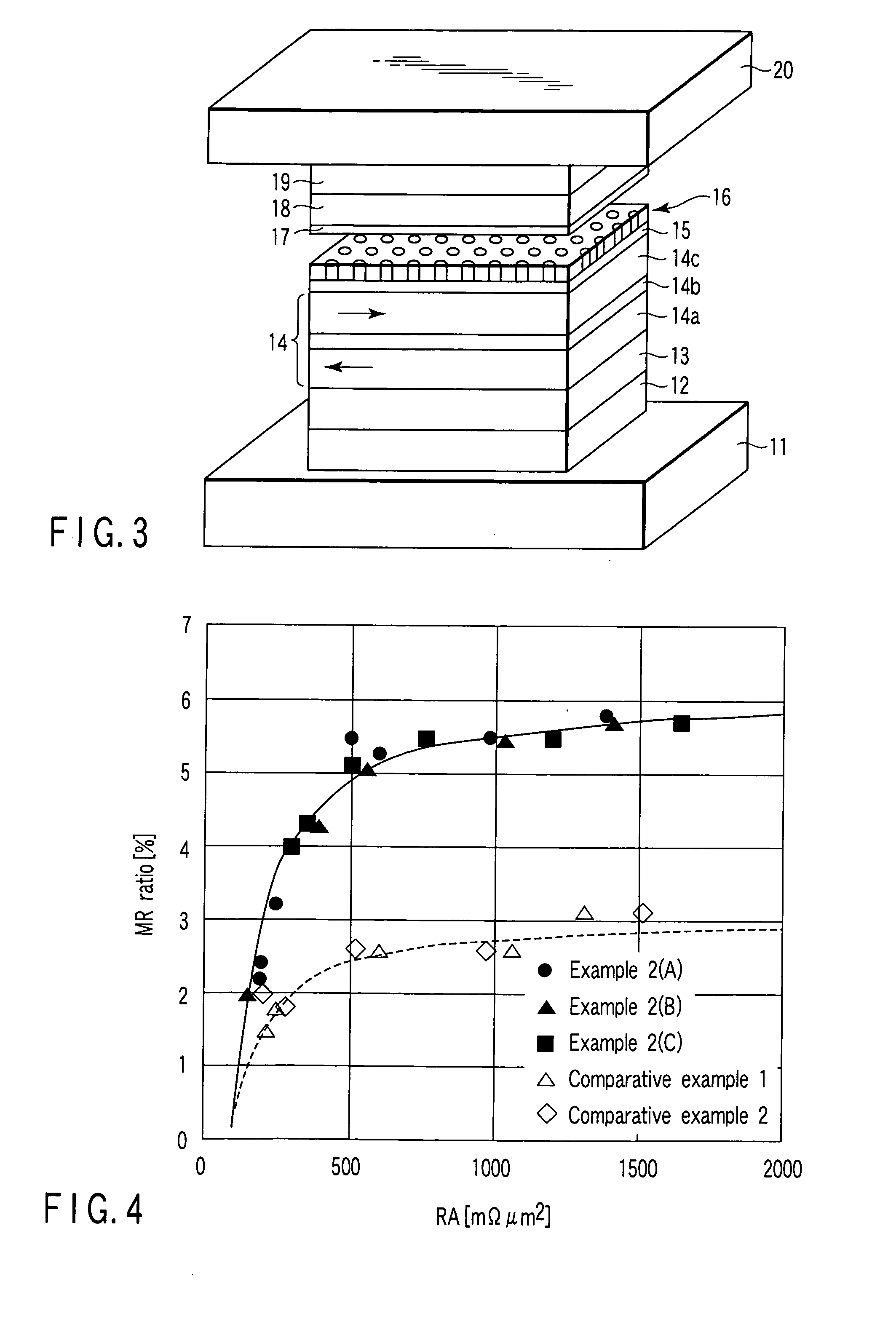
[0050] In this Example, a magnetoresistive element having a stacked structure shown in FIG. 3 is fabricated in the following stacked structure:

[0051] lower electrode 11,

[0052] underlayer 12: Ta [5 nm] / Ru [2 nm],

[0053] pinning layer 13: Pt50Mn50 [15 nm],

[0054] pinned layer 14: Co90Fe10 [3.6 nm] / Ru [0.9 nm] / {(Fe50Co50 [1 nm] / Cu [0.25 nm])×2 / Fe50Co50 [1 nm]},

[0055] metal layer 15: Cu [0.5 nm],

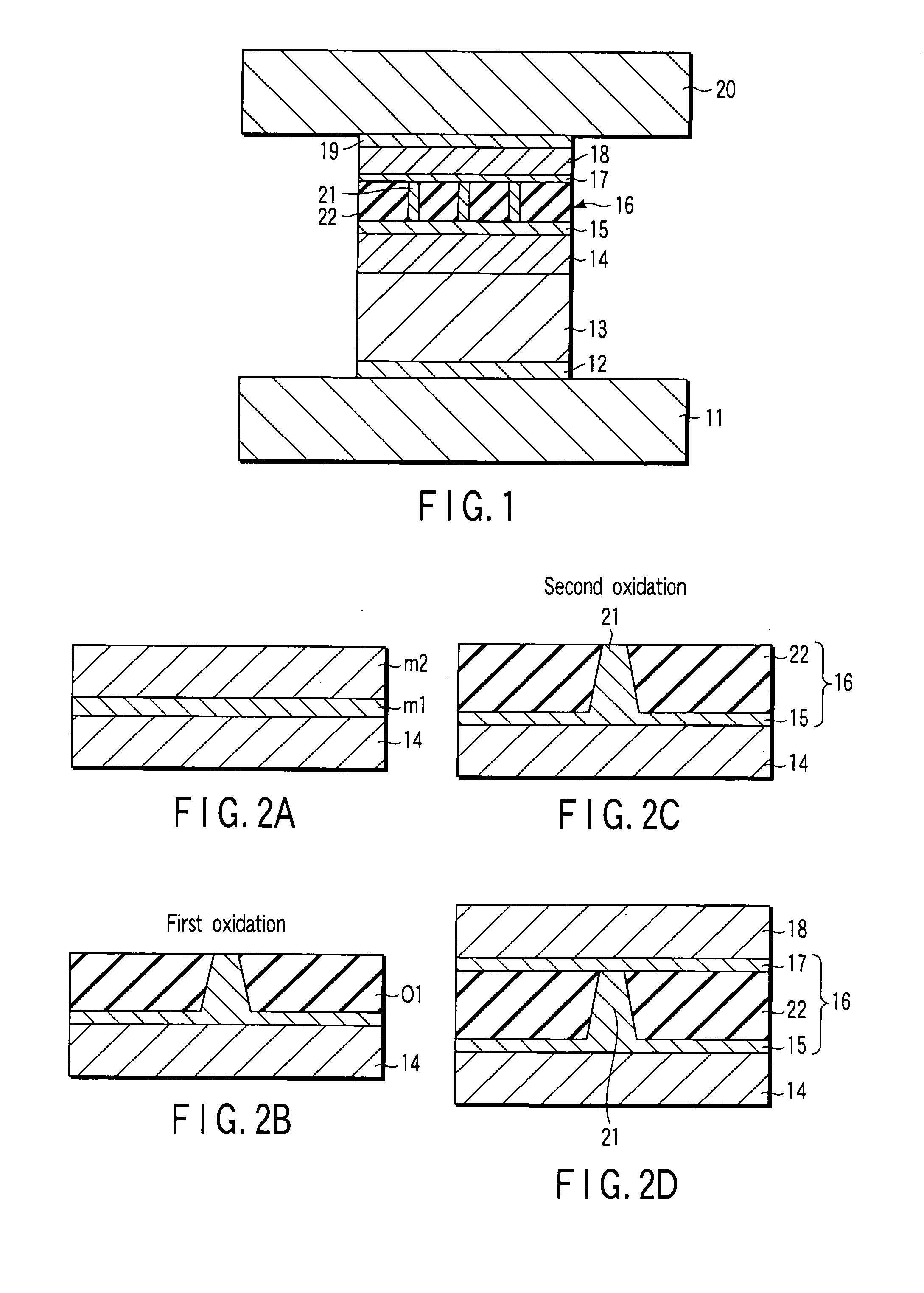
[0056] spacer layer 16: Al2O3 insulating layer 22 and Cu current paths 21 (produced by depositing Al90Cu10 [1 nm] and then performing first and second oxidation treatments),

[0057] metal layer 17: Cu [0.25 nm],

[0058] free layer 18: Co90Fe10 [1 nm] / Ni83Fe17 [3.5 nm],

[0059] cap layer 19: Cu [1 nm] / Ta [5 nm],

[0060] upper electrode 20.

[0061] The lower electrode 11 for supplying a sense current in the direction perpendicular to the spin valve film is formed on the substrate. Ta [5 nm] and Ru [2 nm] are deposited on the lower electrode 11 as the underlayer 12. The Ta layer is a buffer layer th...


PUM

PropertyMeasurementUnit
accelerating voltageaaaaaaaaaa

Abstract

There is provided a method for manufacturing a magnetoresistive element having a magnetization pinned layer, a magnetization free layer, and a spacer layer including an insulating layer arranged between the magnetization pinned layer and the magnetization free layer and current paths passing through the insulating layer. The method includes, in producing the spacer layer, depositing a first non-magnetic metal layer forming the current paths, depositing a second metal layer to be converted into the insulating layer on the first non-magnetic metal layer, and performing two stages of oxidation treatments in which a partial pressure of an oxidizing gas in a first oxidation treatment is set to 1/10 or less of a partial pressure of an oxidizing gas in a second oxidation treatment, and the second metal layer being irradiated with an ion beam or a RF plasma of a rare gas in the first oxidation treatment.

Description

CROSS-REFERENCE TO RELATED APPLICATIONS [0001] This application is based upon and claims the benefit of priority from prior Japanese Patent Application No. 2005-306975, filed Oct. 21, 2005, the entire contents of which are incorporated herein by reference. BACKGROUND OF THE INVENTION [0002] 1. Field of the Invention [0003] The present invention relates to a method for manufacturing a magnetoresistive element having a structure in which a sense current is supplied perpendicularly to the plane of the magnetoresistive film. [0004] 2. Description of the Related Art [0005] In recent years, reduction in size and increase in density of hard disk drive (HDD) are rapidly improved, and this trend will be accelerated in the near future. In order to improve the density of HDD, it is necessary to reduce the width of the recording track to increase the track density. However, the decrease in track width leads to reduction in size of the recorded magnetization, i.e., in magnitude of recording sign...

Claims


Application Information

Patent Timeline
Patent Type & Authority Applications(United States)
IPC IPC(8): B05D5/12
CPCB82Y10/00H01F10/3259B82Y40/00C23C8/02C23C8/34G11B5/3163G11B5/3932G11B2005/3996H01F10/3268H01F41/305C23C28/321C23C28/322C23C28/34C23C28/345C23C28/3455C23C28/42B82Y25/00
Inventor FUJI, YOSHIHIKOFUKUZAWA, HIDEAKIYUASA, HIROMIIWASAKI, HITOSHI
Owner KK TOSHIBA
Why Eureka
Try Eureka