Methods for forming germanium-on-insulator semiconductor structures using a porous layer and semiconductor structures formed by these methods

a technology of germanium-on-insulator and semiconductor structure, which is applied in the field of method of forming germanium-on-insulator semiconductor structure and semiconductor structure formed by these methods, can solve the problems of defective active layer for device formation, limited process throughput, and significant density of threading dislocations, so as to minimize the nucleation of threading dislocations

Inactive Publication Date: 2007-04-26
GLOBALFOUNDRIES INC
View PDF18 Cites 72 Cited by
  • Summary
  • Abstract
  • Description
  • Claims
  • Application Information

AI Technical Summary

Benefits of technology

[0012] The germanium-containing layer, which may be pure monocrystalline germanium, may be deposited directly on the porous layer because stress arising from the lattice mismatch between silicon and germanium is relaxed by the porous material, such as

Problems solved by technology

There are several drawbacks associated with this conventional approach for forming GOI substrates.
Growing a buffer layer of sufficient thickness to accomplish this objective requires an extensively long process duration and, therefore, the process throughput is limited.
Second, a significant density of threading dislocations may nevertheless propagate from the buffer layer into the relaxed layer during epitaxial growth and/or during the subsequent thermal process.
These threading dislocations may continue to propagate into the germanium layer, which resu

Method used


Image

  • Methods for forming germanium-on-insulator semiconductor structures using a porous layer and semiconductor structures formed by these methods
  • Methods for forming germanium-on-insulator semiconductor structures using a porous layer and semiconductor structures formed by these methods
  • Methods for forming germanium-on-insulator semiconductor structures using a porous layer and semiconductor structures formed by these methods

Examples


Embodiment Construction

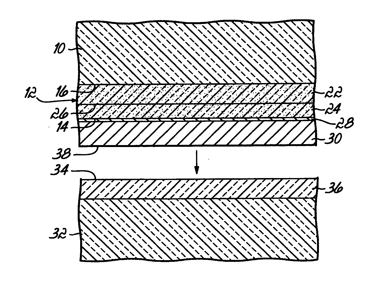
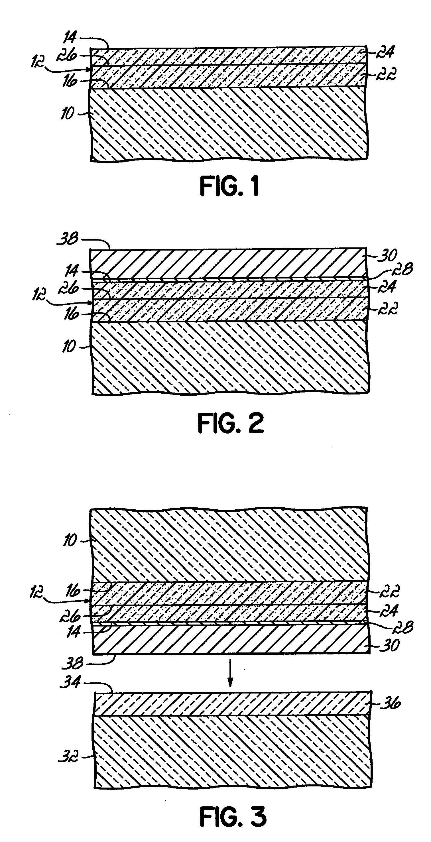
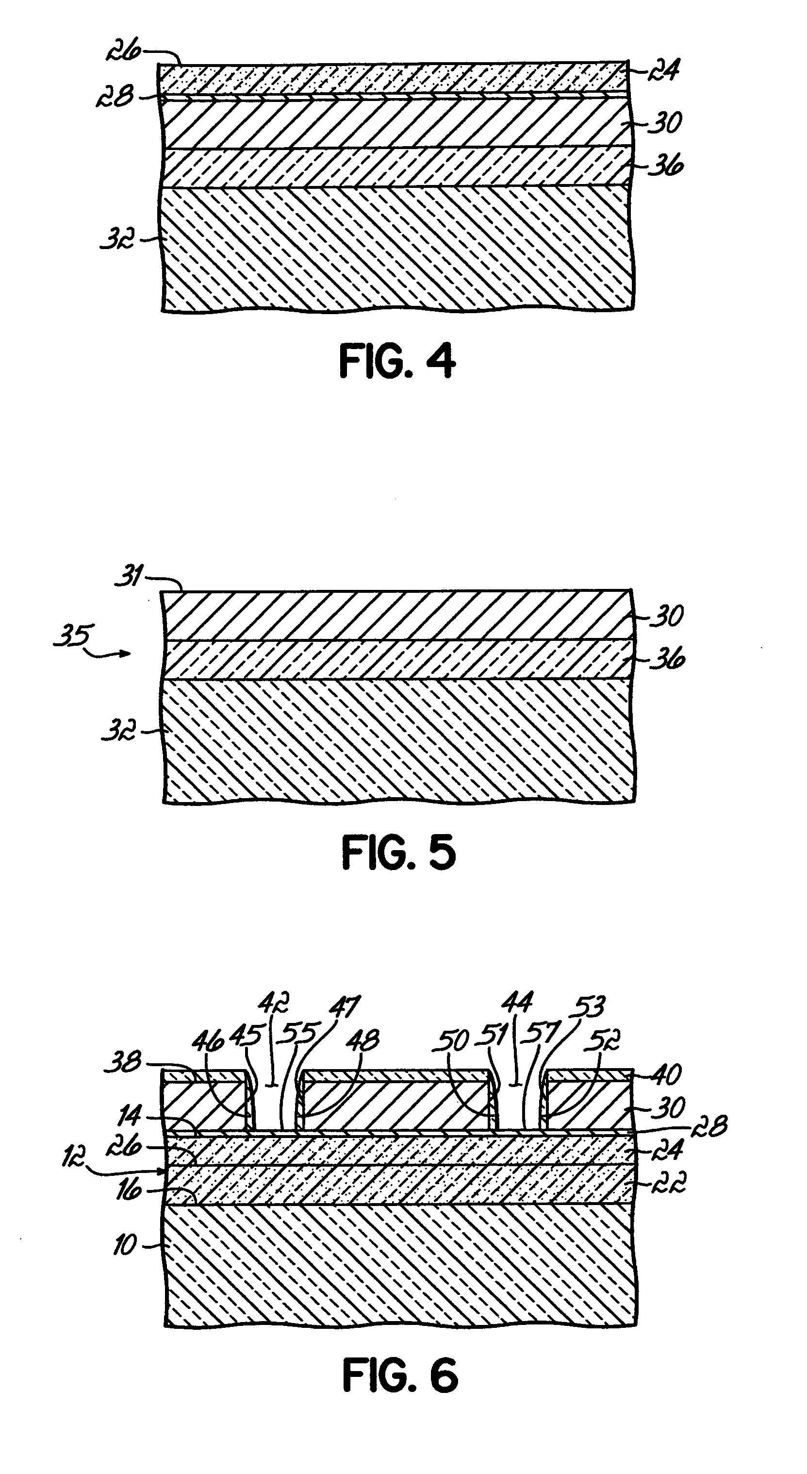
[0017] The present invention provides a semiconductor structure that may be used as a germanium-on-insulator (GOI) substrate for device fabrication. The GOI substrate of the present invention may be particularly advantageous for forming complementary metal oxide semiconductor field effect transistors (CMOSFETs) as a substitute for, or complement to, conventional silicon-on-insulator (SOI) substrates. Germanium (Ge) advantageously has a significantly higher carrier mobility than silicon (Si) for both electrons and holes, as well as lower contact resistance and lower dopant activation temperatures that facilitate the formation of shallow junctions. The present invention will now be described in greater detail by referring to the drawings that accompany the present application.

[0018] With reference to FIG. 1, a porous layer 12 is formed on a first substrate 10. Substrate 10 may be a bulk silicon substrate, in which instance the porous layer 12 represents a depth over which the constit...


PUM


Abstract

A semiconductor structure that includes a monocrystalline germanium-containing layer, preferably substantially pure germanium, a substrate, and a buried insulator layer separating the germanium-containing layer from the substrate. A porous layer, which may be porous silicon, is formed on a substrate and a germanium-containing layer is formed on the porous silicon layer. The porous layer may be converted to a layer of oxide, which provides the buried insulator layer. Alternatively, the germanium-containing layer may be transferred from the porous layer to an insulating layer on another substrate. After the transfer, the insulating layer is buried between the latter substrate and the germanium-containing layer.

Description

FIELD OF THE INVENTION [0001] The invention relates generally to semiconductor structures and methods and, in particular, to methods for forming germanium-on-insulator semiconductor structures and semiconductor structures formed by these methods. BACKGROUND OF THE INVENTION [0002] Germanium-on-insulator (GOI) substrates may play an important role in future complementary metal oxide semiconductor (CMOS) scaling. In the semiconductor community, germanium (Ge) is widely recognized as having higher carrier mobility than silicon (Si) for both electrons and holes, as well as lower contact resistance and lower dopant activation temperatures that facilitate the formation of shallow junctions. The development of high-k dielectrics with a dielectric constant greater than silicon oxide (SiO2) for use as a gate insulator in metal oxide semiconductor field effect transistors (MOSFETs) is expected to provide a solution to the general poor quality of germanium oxide, which has historically represe...

Claims


Application Information

Patent Timeline
IPC IPC(8): H01L21/30H01L21/20H01L21/76
CPCH01L21/76245H01L21/76251Y10S438/933
Inventor CHENG, KANGGUOGREENE, BRIAN JOSEPHMANDELMAN, JACK ALLAN
Owner GLOBALFOUNDRIES INC
Why Eureka
Try Eureka