Electrode structure and optical semiconductor element

a technology of optical semiconductor elements and electrode structures, applied in semiconductor lasers, lasers, solid-state devices, etc., can solve the problems of reducing the yield in the manufacturing process, difficult to directly connect the first electrode to the upper surface of the second conductive layer, and the disconnection defect, so as to reduce the yield in the process of forming the optical semiconductor element and suppress the reduction in the yield. , the effect of reducing the electrostatic breakdown voltage of the laser resonator against a revers

Inactive Publication Date: 2007-05-03
SEIKO EPSON CORP
View PDF1 Cites 6 Cited by
  • Summary
  • Abstract
  • Description
  • Claims
  • Application Information

AI Technical Summary

Benefits of technology

[0020] In accordance with the present embodiment, one end of the first electrode can be prevented from forming an inversely tapered shape, like the embodiment described above, whereby disconnection of the third electrode to be formed on the first electrode can be avoided. Furthermore, a reduction in the yield in the process of forming the optical semiconductor element can be suppressed.
[0021] It is noted that, if the upper surface of the laser resonator and the terminal electrode are connected with each other by the first electrode, and the upper surface of the laser resonator and the upper surface of the additional element are connected with each other by the first electrode, diffusion may occur between the first electrode and the upper surface of the additional element, which may cause unexpected functional deterioration of the additional element. For this reason, it is difficult to directly connect the first electrode to the upper surface of the additional element. Therefore, when the upper surface of the laser resonator and the terminal electrode are to be conductively connected with each other through the upper surface of the additional element, it is necessary to connect them with a third electrode that does not exhibit any conductivity type. According to the present embodiment, disconnection of the third electrode to be provided in such a case as described above can be effectively prevented.
[0022] In the optical semiconductor element in accordance with an aspect of the embodiment of the invention, the insulation layer may preferably be formed with another sloped section that gradually slopes down toward the upper surface of the second columnar structure, and the marginal end of the second electrode may preferably be formed on the other sloped section. According to the present embodiment, like the embodiment described above, the marg

Problems solved by technology

It is believed that, because the end of the ring-shaped electrode has an inversely tapered shape due to the burr, the portion in the inversely tapered shape functions as a mask when the lead-out electrode is formed, thereby causing the disconnection defect.
For this reason, disconnection of lead-out electrodes causes to lower the yield in the manufacturing process.
For this reason, it is difficult to directly connect the first electrode to the upper surface of the second conductive layer.
It is noted that, if the upper surface of the first columnar structure and the terminal electrode are connected with each other by the first electrode, and the upper surface of the first columnar structure and the upper surface of the second columnar structure are connected with each other by the first electrode, diffusion may occur between the first electr

Method used


Image

  • Electrode structure and optical semiconductor element
  • Electrode structure and optical semiconductor element
  • Electrode structure and optical semiconductor element

Examples


first embodiment

[0041] First Embodiment

[0042] Structure of Optical Semiconductor Element

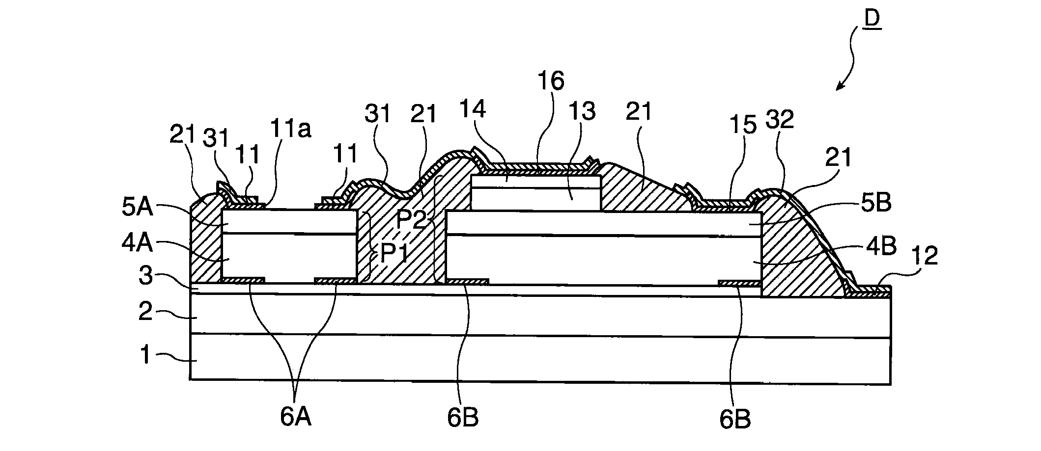
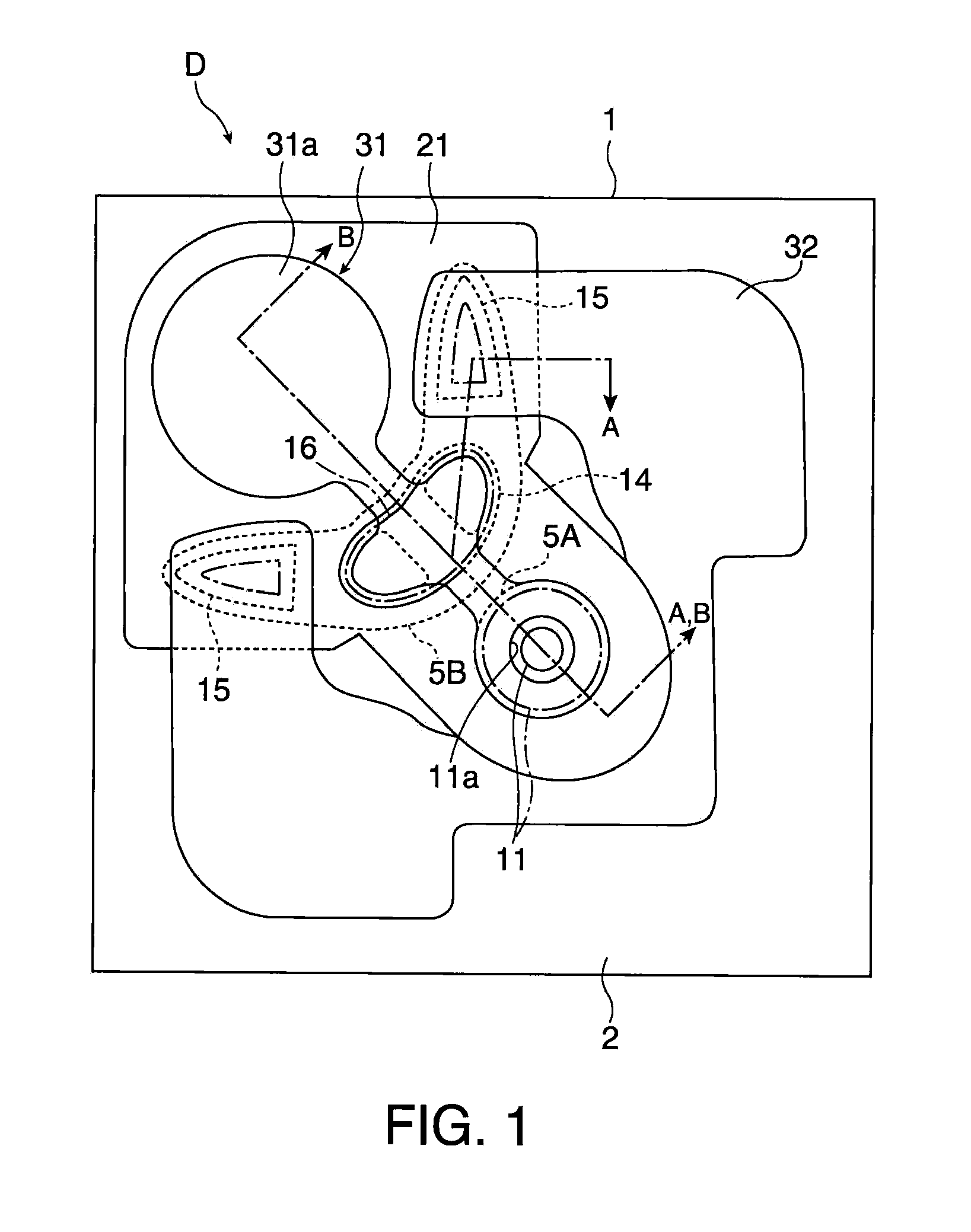
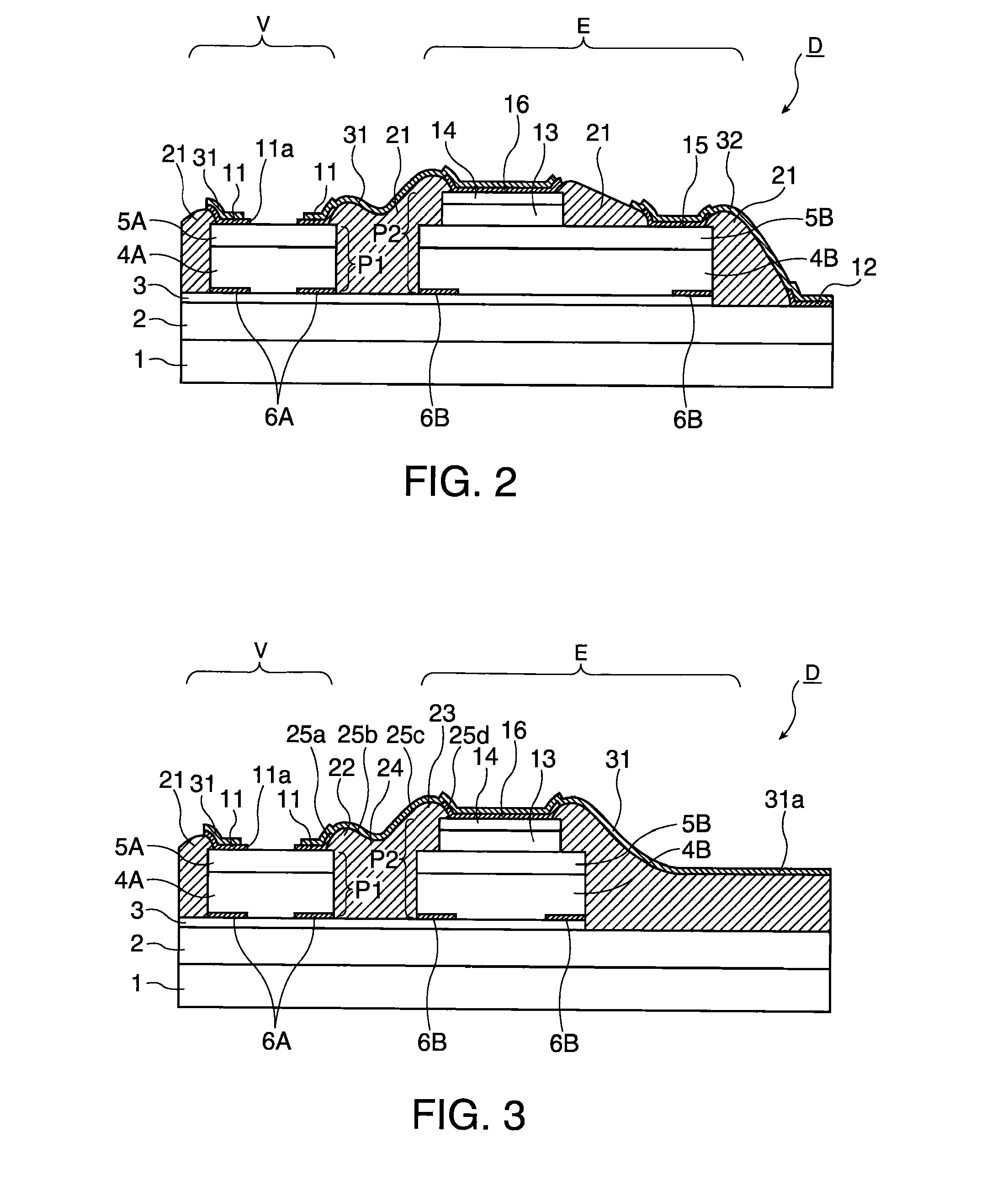
[0043] First, a first embodiment of the invention is described with reference to the accompanying drawings. FIG. 1 is a schematic plan view of an optical semiconductor element D in accordance with the first embodiment of the invention. FIG. 2 is a cross-sectional view taken along a line A-A of FIG. 1, FIG. 3 is a cross-sectional view taken along a line B-B of FIG. 1, FIG. 4 is a partially enlarged view of FIG. 3, and FIG. 5 is an equivalent circuit diagram of FIG. 1. As shown in FIG. 1 through FIG. 3, the optical semiconductor element D is equipped with a surface-emitting type semiconductor laser V and a rectification diode (additional element) E.

[0044] Surface-Emitting Type Semiconductor Laser

[0045] As shown in FIG. 1 through FIG. 3, the surface-emitting type semiconductor laser V is formed on a substrate 1, for example, a semiconductor substrate composed of n-type GaAs. The surface-emitting type semiconduct...

second embodiment

[0078] Second Embodiment

[0079] Structure of Optical Semiconductor Element

[0080] Next, a second embodiment of the invention is described with reference to the accompanying drawings. In the following description, components that are the same as those described above in the first embodiment are appended with the same reference numbers, and their description is omitted. FIG. 10 is a schematic plan view of an optical semiconductor element D′, FIG. 11A is a cross-sectional view taken along a line C-C of FIG. 10, and FIG. 11B is a partially enlarged view of FIG. 11A. The second embodiment is different from the first embodiment in that the optical semiconductor element D′ of the second embodiment is composed of a surface-emitting type semiconductor laser V′ alone.

[0081] The surface-emitting type semiconductor laser V′ has a multilayer structure in which a first mirror layer 2, an active layer 3 and a second mirror layer 4 are sequentially laminated, thereby forming a first columnar sectio...


PUM


Abstract

An electrode structure includes a first conductive layer, an insulation layer that covers at least a portion of a marginal area of an upper surface of the first conductive layer and has a first sloped section that slopes down toward the upper surface of the first conductive layer, a first electrode having one end formed on the first conductive layer and another end formed on the first sloped section, a third electrode that is formed on the first electrode and the insulation layer, and covers the another end of the first electrode.

Description

[0001] The entire disclosure of Japanese Patent Application Nos: 2005-312506, filed Oct. 27, 2005 and 2006-171150, filed Jun. 21, 2006 are expressly incorporated by reference herein. BACKGROUND [0002] 1. Technical Field [0003] The present invention relates to electrode structures and optical semiconductor elements. [0004] 2. Related Art [0005] A surface-emitting type semiconductor laser is one type of optical elements that emit laser light. The surface-emitting type semiconductor laser is provided with a laser resonator formed in a direction orthogonal to a surface of the substrate, and emits laser light from an upper surface of the laser resonator. In the surface-emitting type semiconductor laser, surfaces around the columnar laser resonator provided on the surface of the substrate may be coated and planarized with an insulation material such as polyimide. For example, Japanese Laid-open patent application JP-A-2004-288971 is an example of related art. [0006] A structure of a surfa...

Claims


Application Information

Patent Timeline
IPC IPC(8): H01L33/00H01L21/00
CPCB82Y20/00H01S5/0261H01S5/0425H01S5/06825H01S5/18311H01S5/3432H01S2301/176H01L2224/24H01L2224/73267H01L2224/24137H01L2224/92244H01L2224/82H01S5/04256H01S5/04257H01S5/02345
Inventor SATO, ATSUSHI
Owner SEIKO EPSON CORP
Why Eureka
Try Eureka