

Method for forming multi-layer bumps on a substrate
a multi-layer bump and substrate technology, applied in the direction of printed circuit aspects, lithographic masks, non-printed masks, etc., can solve the problems of chemical waste, chemical waste, and need for removing the photoresist layer by chemical solutions
- Summary
- Abstract
- Description
- Claims
- Application Information
AI Technical Summary
Benefits of technology
Problems solved by technology
Method used
Image

Examples
Embodiment Construction
[0016] A method for forming multi-layer bumps or connectors on a substrate in a semiconductor chip or printed circuit board (PCB) environment is provided. In the following description, numerous specific details are set forth in order to provide a thorough understanding of the present invention. It will be understood, however, to one skilled in the art, that the present invention may be practiced without some or all of these specific details. In other instances, well known process operations have not been described in detail to not unnecessarily obscure the present invention.
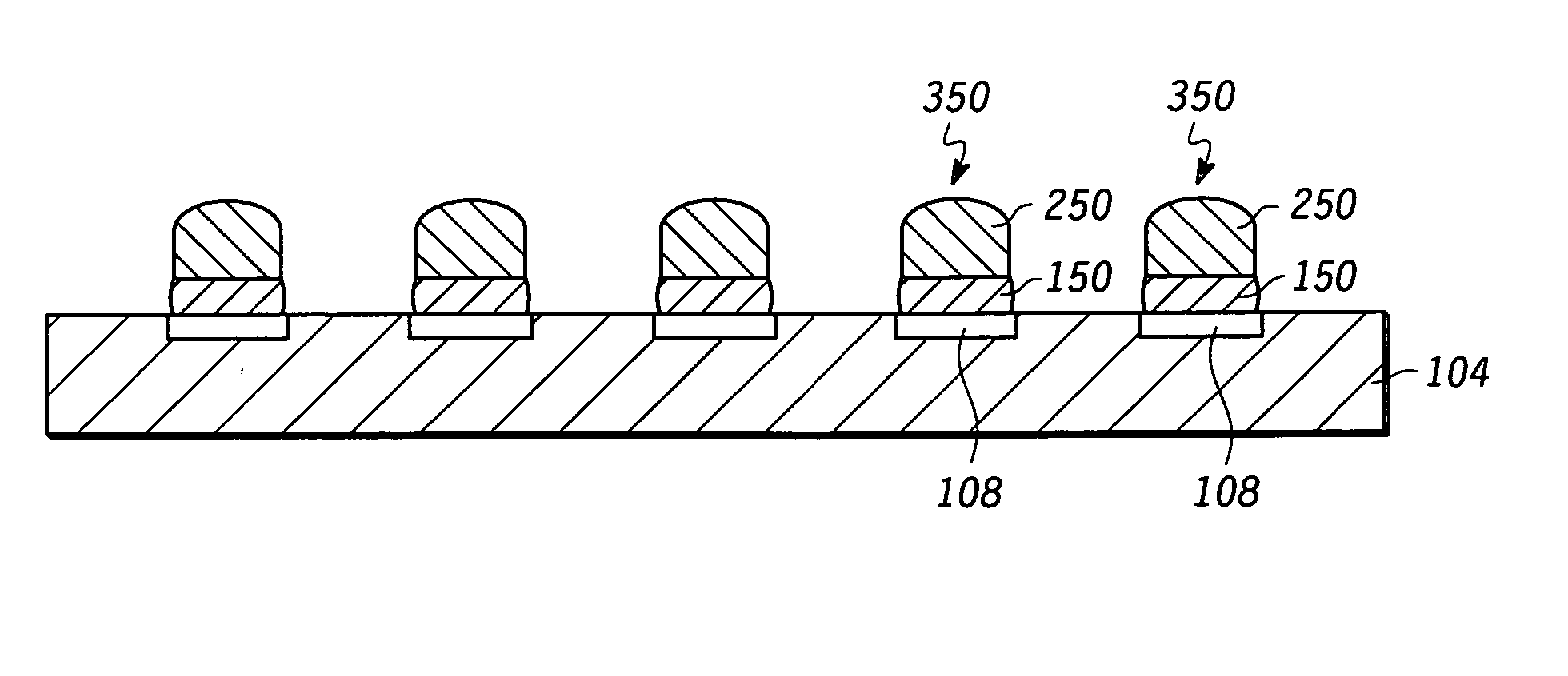
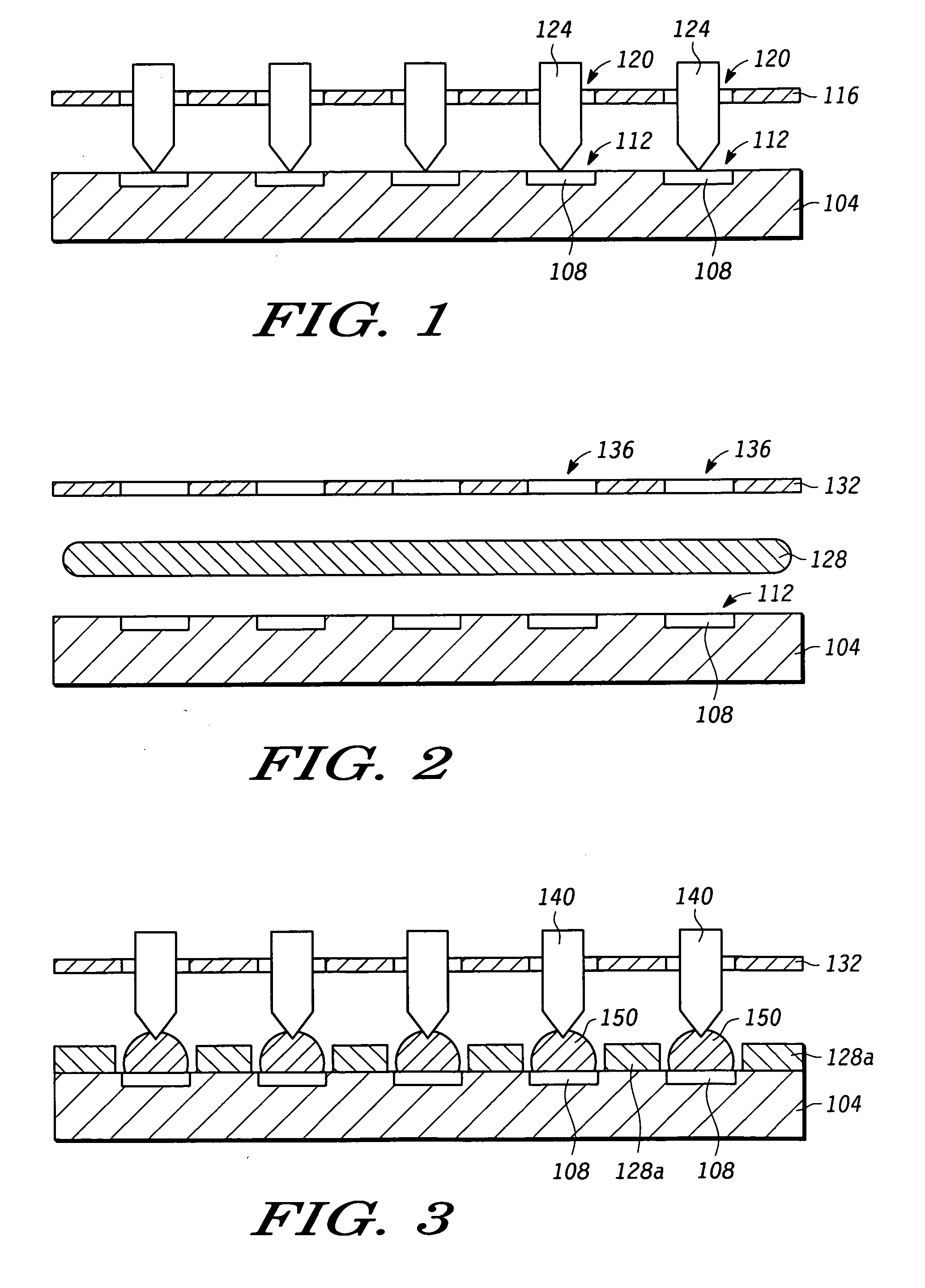
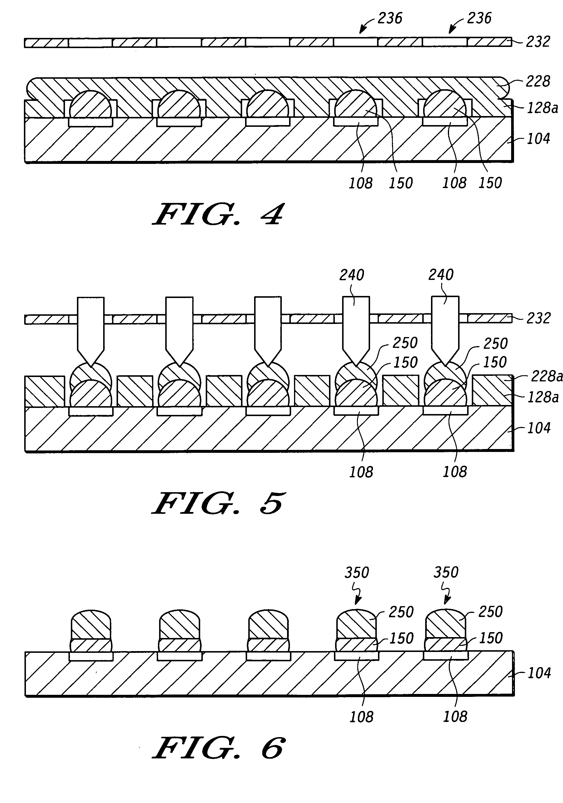
[0017] Referring now to FIG. 1, an enlarged, cross-sectional view of a semiconductor chip or wafer or PCB substrate 104 in accordance with one embodiment of the present invention is shown. The substrate 104 includes a number of bond pads 108 for defining bump sites 112 on which bumps may be formed. Before forming the bumps, the substrate 104 is cleaned to remove contaminants, such as aluminum oxide, from the bon...
PUM
| Property | Measurement | Unit |
|---|---|---|
| particle size | aaaaa | aaaaa |
| melting point | aaaaa | aaaaa |
| melting point | aaaaa | aaaaa |
Abstract
Description
Claims
Application Information