Method of reforming reformable members of an electronic package and the resultant electronic package

a technology of electronic packages and reformable members, applied in the field of electronic packages, can solve the problems of adversely affecting reliability, solder connections between a chip and a circuitized substrate are subject to thermally-induced stresses, and the thermal expansion characteristics of the two objects being connected may differ substantially, so as to improve the standoff capability and improve the reliability of the package

Inactive Publication Date: 2003-06-24
INVENSAS CORP
View PDF18 Cites 22 Cited by
  • Summary
  • Abstract
  • Description
  • Claims
  • Application Information

AI Technical Summary

Benefits of technology

An object of the present invention is to provide an electronic package having an improved standoff capability to provide improved package reliability.
The invention is adaptable to mass production and will provide significant improvement in the ability to manufacture high reliability electronic packages, having a high standoff from the substrate to which the packages are assembled.

Problems solved by technology

An inherent problem with either the C4 or BGA connection is that the thermal expansion characteristics of the two objects being connected may differ substantially.
Therefore, the solder connections between a chip and circuitized substrate will be subject to thermally-induced stresses.
In a similar manner, thermal expansion mismatch between a chip carrier package and a circuit card or board may give rise to significant stresses which adversely affect reliability.
Each of these methods helps to form reliable connections, but at a cost of manufacturability, restrictive material choice, or other disadvantage.
The use of a solder-coated copper ball as a standoff-enhancement device results in a higher standoff, but greatly increased joint stiffness.
The manufacturability difficulties of the solder column connection method limit the pitch (distance between adjacent columns) of a package interconnection to about 1.0 millimeter (mm) at the present time, and require the use of a hierarchy of solder melt materials.

Method used


Image

  • Method of reforming reformable members of an electronic package and the resultant electronic package
  • Method of reforming reformable members of an electronic package and the resultant electronic package
  • Method of reforming reformable members of an electronic package and the resultant electronic package

Examples


Embodiment Construction

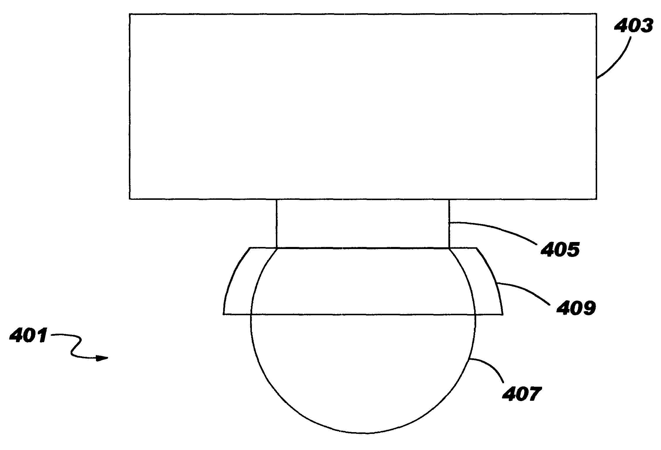
Referring now to the drawings in detail, FIGS. 3-5 illustrate a process for making an electronic package according to one embodiment of the present invention. The electronic package 301 comprises a substrate 303, a contact pad 305, and a reformable ball 307. By way of example, reformable ball 307 is a solder ball. An elastic sleeve 309 is formed from rubber, plastic or a shaped memory alloy and is initially apart from electronic package 301. When relaxed, an inner diameter (shown in phantom) of elastic sleeve 309 is less than an outer diameter of reformable solder ball 307. In FIG. 4, elastic sleeve 309 has been positioned around reformable solder ball 307 by stretching the elastic sleeve from its relaxed state to an unrelaxed state conforming to the outside diameter of the reformable solder ball 307. To ease application of the elastic sleeve, a lubricant such as a solder flux may be employed. A girdling (or squeezing) pressure now exists between elastic sleeve 309 and reformable so...


PUM

PropertyMeasurementUnit
transition temperatureaaaaaaaaaa
glass transition temperatureaaaaaaaaaa
glass transition temperaturesaaaaaaaaaa

Abstract

An electronic package includes a substrate having a contact pad thereon, a reformable member such as a solder ball positioned on the contact pad, and an elastic member positioned around the reformable member. The elastic member exerts a girdling force on the reformable member so that when the reformable member is softened, the elastic member elongates the reformable member. This elongation accommodates thermal and other stresses between the foregoing substrate and another substrate joined at the free end of the reformable member. An apparatus is also provided for positioning the elastic member on and around the reformable member.

Description

The invention relates generally to electronic packages and more particularly to assemblies for connection of integrated circuit chips to chip carriers, chip carriers to printed circuit boards, modules to printed circuit cards, and the like.Various ceramic ball grid array packages, leadless chip carriers, laminated chip carriers, tape ball grid array packages, and overmolded, globtop, and plastic ball grid array packages are known today. Such packages typically contain a semiconductor device (a chip) and provide for electrical and thermal connection paths to and from the chip, while protecting the chip from extraneous environmental factors, processing chemicals, and handling.Such packages typically include connections known in the art as solder reflow (or melt) connections. These connections provide for both electrical and thermal conduction paths. It is known from prior art that a reformable solder ball 107 can be attached to contact pad 105 on substrate 103 of electronic package 10...

Claims


Application Information

Patent Timeline
Patent Type & Authority Patents(United States)
IPC IPC(8): H05K3/34H05K13/04
CPCH05K3/3436H05K13/0465H01L2224/10126H01L2924/09701H05K2201/0133H05K2201/10265Y10T29/49204H05K2203/043H05K2203/0465H05K2203/306H01L2924/01322Y10T29/49211Y10T29/49213H05K2201/10977H01L24/05H01L2224/05568H01L2224/05573H01L2224/056Y02P70/50H01L2924/00014
Inventor ALCOE, DAVID J.
Owner INVENSAS CORP
Why Eureka
Try Eureka