Discharge light-emitting device
a discharge light and light-emitting device technology, which is applied in the direction of gas-filled discharge tubes, discharge tubes/lamp details, gas plasma lamps, etc., can solve the problems of insufficient use of cathode lamps, limited life span of discharge lamps, and gradual decrease of lamp efficiency
- Summary
- Abstract
- Description
- Claims
- Application Information
AI Technical Summary
Problems solved by technology
Method used
Image

Examples
first embodiment
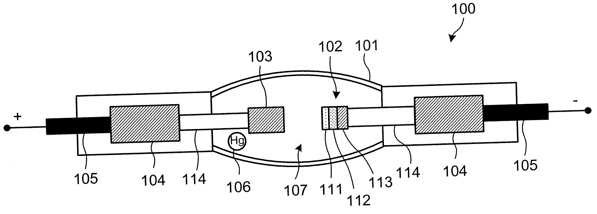
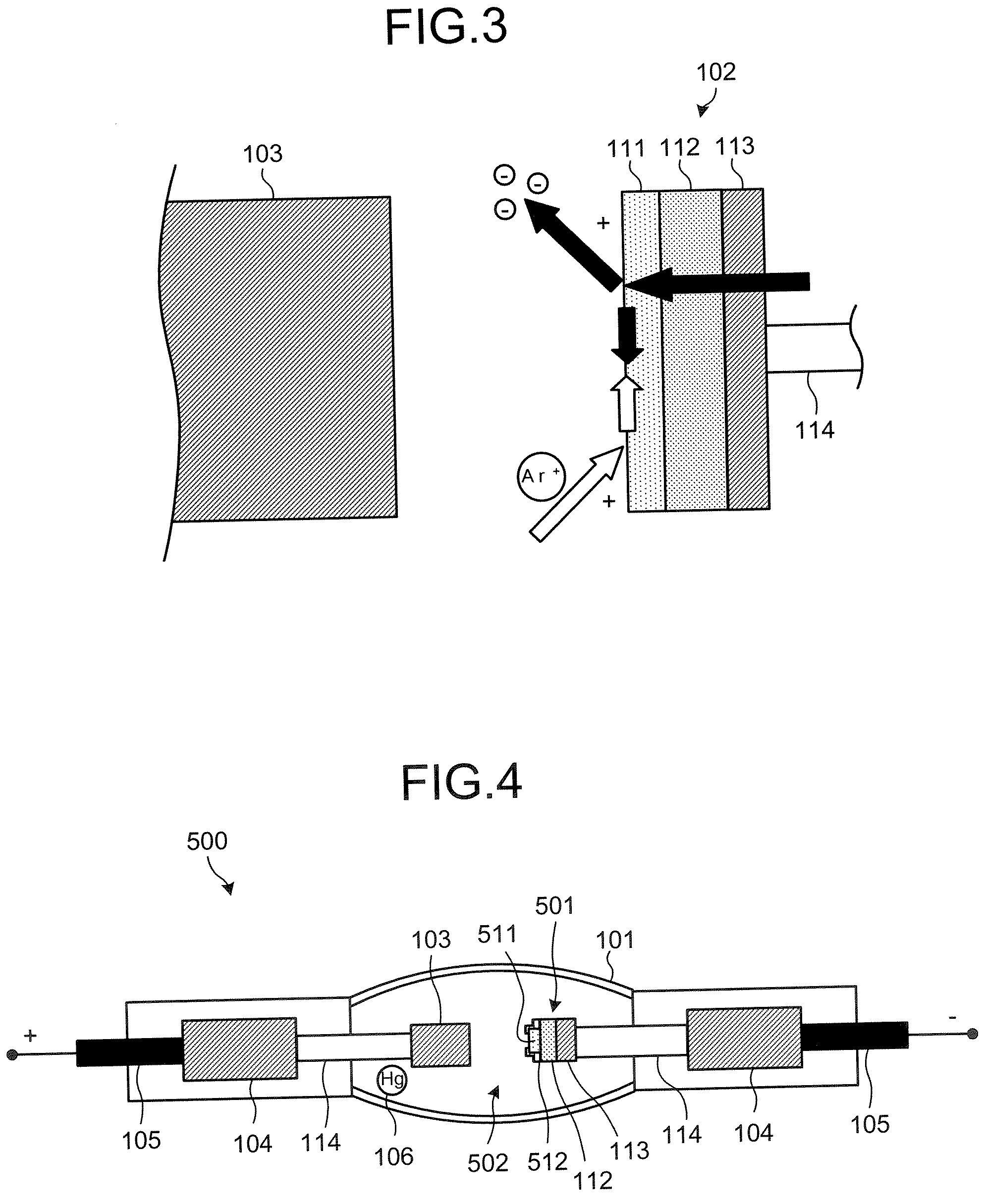
[0056] The discharge gas 502 contains argon gas (Ar) and a trace of halogen gas similar to those in the first embodiment above, and the discharge gas 502 further contains a trace of hydrogen. The reason for containing the hydrogen will be explained later.
[0057] The cathode 501 is configured by the electrically conductive substrate 113, the n-type semiconductor layer 112 that is provided on the electrically conductive substrate 113, a p-type semiconductor layer 511 that is provided on a top of the n-type semiconductor layer 112, and an insulating layer 512 that covers the junction of the p-type semiconductor layer 511 and the n-type semiconductor layer 112; and the n-type semiconductor layer 112 and the p-type semiconductor layer 511 form a pn junction. Further, the surface of the p-type semiconductor layer 511 is hydrogen-terminated.
[0058] The p-type semiconductor layer 511 differs from the p-type semiconductor layer 111 according to the first embodiment since the p-type semiconduc...
second embodiment
[0060]FIG. 5 is a cross-sectional view schematically showing the anode 103 and a cathode 601 according to an embodiment different from the present embodiment to explain the discharge light-emitting device 500 of the The cathode 601 includes the electrically conductive substrate 113, the n-type semiconductor layer 112 that is provided on the electrically conductive substrate 113, and a p-type semiconductor layer 611 that is provided on the n-type semiconductor layer 112, and the surface of the p-type semiconductor layer 611 is hydrogen-terminated. The hydrogen-termination of the surface of the p-type semiconductor layer 611 causes the electron affinity to decrease, thereby resulting in the negative electron affinity of the surface of the p-type semiconductor layer 611.
[0061] In the embodiment shown in FIG. 5, the outer envelope 101 (not shown) is filled with the discharge gas 502 containing a trace of hydrogen. Thus, the hydrogen termination occurs and is maintained at the surface o...
third embodiment
[0097] The exposed portion to the discharge space at the junction of the n-type semiconductor layer 912 and the p-type semiconductor layer 911 is insulated in the discharge light-emitting device 1100 according to the present embodiment. Consequently, the electrode 1101 of the discharge light-emitting device 1100 can prevent the formation of short-circuit by the hydrogen termination at the pn junction. Further, the electrode 1101 of the discharge light-emitting device 1100 can hydrogen-terminate the p-type semiconductor layer 911 by a trace of hydrogen contained in the discharge gas 1102. Consequently, the electrode 1101 is provided with the hydrogen-terminated p-type semiconductor layer 911 having negative electron affinity as the electron emissive surface. Further, the electrode 1101 works as cathode and anode. Consequently, the similar effect to the discharge light-emitting device 900 of the third embodiment described above can be obtained, and the discharge efficiency is further ...
PUM
 Abstract
Description
Claims
Application Information
 - R&D
- Intellectual Property
- Life Sciences
- Materials
- Tech Scout
- Unparalleled Data Quality
- Higher Quality Content
- 60% Fewer Hallucinations
Browse by: Latest US Patents, China's latest patents, Technical Efficacy Thesaurus, Application Domain, Technology Topic, Popular Technical Reports.
© 2025 PatSnap. All rights reserved.Legal|Privacy policy|Modern Slavery Act Transparency Statement|Sitemap|About US| Contact US: help@patsnap.com