Spacer Electrode Small Pin Phase Change Memory RAM and Manufacturing Method

Active Publication Date: 2007-05-17
MACRONIX INT CO LTD
View PDF5 Cites 228 Cited by
  • Summary
  • Abstract
  • Description
  • Claims
  • Application Information

AI Technical Summary

Benefits of technology

[0012] The active volume of memory material subject of programmable resistance can be very small, determined by the thickness of the insulating wall (path length in the x-direction), the thickness of the thin film used to form the bridge (y-direction), the width of the bridge orthogonal to the path length (z-direction), and the width of the side wall electrode structures acting as contacts to the bridge. The width of the side wall electrode structures and the thickness of the thin film of memory material used to form the bridge are determined in embodiments of the technology by thin film thicknesses which are not limited by the lithographic processes used in manufacturing the memory cell. The width of the bridge and the thickness of the insulation wall are also smaller than a minimum feature size F that is specified for a lithographic process

Problems solved by technology

Problems have arisen in manufacturing such devices with very small dimensions, and with va

Method used


Image

  • Spacer Electrode Small Pin Phase Change Memory RAM and Manufacturing Method
  • Spacer Electrode Small Pin Phase Change Memory RAM and Manufacturing Method
  • Spacer Electrode Small Pin Phase Change Memory RAM and Manufacturing Method

Examples


Embodiment Construction

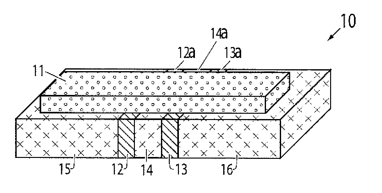
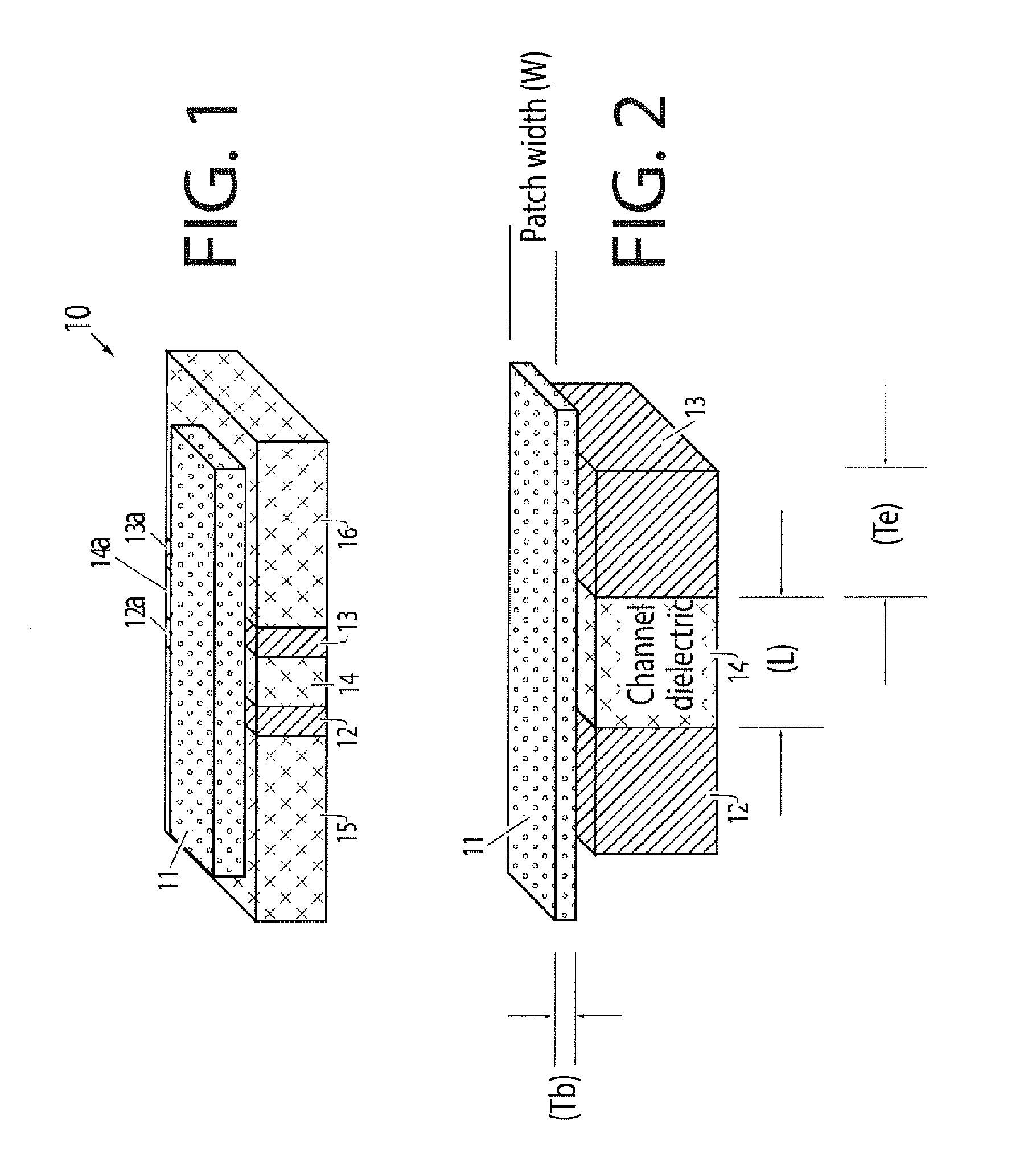
[0057] A detailed description of thin film fuse phase change memory cells, arrays of such memory cells, and methods for manufacturing such memory cells, is provided with reference to FIGS. 1-25.

[0058]FIG. 1 illustrates a basic structure of a memory cell 10 including a bridge 11 of memory material on an electrode layer which comprises a first electrode 12, a second electrode 13, and an insulating wall 14 between the first electrode 12 and the second electrode 13. The first and second electrodes comprise thin film sidewall structures. Insulating fill 15, 16 is adjacent to the sidewall structures, and provides for planarization of the top surface for support of the bridge 11. As illustrated, the first and second electrodes 12, 13 have top surfaces 12a and 13a. Likewise the insulating member 14 has a top surface 14a. The top surfaces 12a, 13a, 14a of the structures in the electrode layer define a substantially planar top surface of the electrode layer in the illustrated embodiment. The...


PUM


Abstract

A memory device comprising a first pan-shaped electrode having a side wall with a top side, a second pan-shaped electrode having a side wall with a top side and an insulating wall between the first side wall and the second side wall. The insulating wall has a thickness between the first and second side walls near the respective top sides. A bridge of memory material crosses the insulating wall, and defines an inter-electrode path between the first and second electrodes across the insulating wall. An array of such memory cells is provided. The bridges of memory material have sub-lithographic dimensions.

Description

RELATED APPLICATION DATA [0001] The present application claims the benefit of U.S. Provisional Patent Application No. 60 / 737,293; entitled SPACER ELECTRODE SMAL PIN PHASE CHANGE RAM AND MANUFACTURING METHOD, filed 16 Nov. 2005.PARTIES TO A JOINT RESEARCH AGREEMENT [0002] International Business Machines Corporation, a New York corporation; Macronix International Corporation, Ltd., a Taiwan corporation, and Infineon Technologies A.G., a German corporation, are parties to a Joint Research Agreement. BACKGROUND OF THE INVENTION [0003] 1. Field of the Invention [0004] The present invention relates to high-density memory devices based on phase change based memory materials, including chalcogenide based materials and on other programmable resistive materials, and to methods for manufacturing such devices. [0005] 2. Description of Related Art [0006] Phase change based memory materials are widely used in read-write optical disks. These materials have at least two solid phases, including for ...

Claims


Application Information

Patent Timeline
IPC IPC(8): B65D85/575
CPCG11C13/0004G11C13/0007G11C13/0014G11C13/0016G11C2213/31G11C2213/79H01L27/2436H01L45/04H01L45/06H01L45/1226H01L45/14H01L45/144H01L45/146H01L45/147H01L45/148H01L45/1675H10B63/30H10N70/231H10N70/20H10N70/823H10N70/881H10N70/884H10N70/8828H10N70/8833H10N70/8836H10N70/063
Inventor LUNG, HSIANG LANCHEN, SHIH HUNG
Owner MACRONIX INT CO LTD
Why Eureka
Try Eureka