

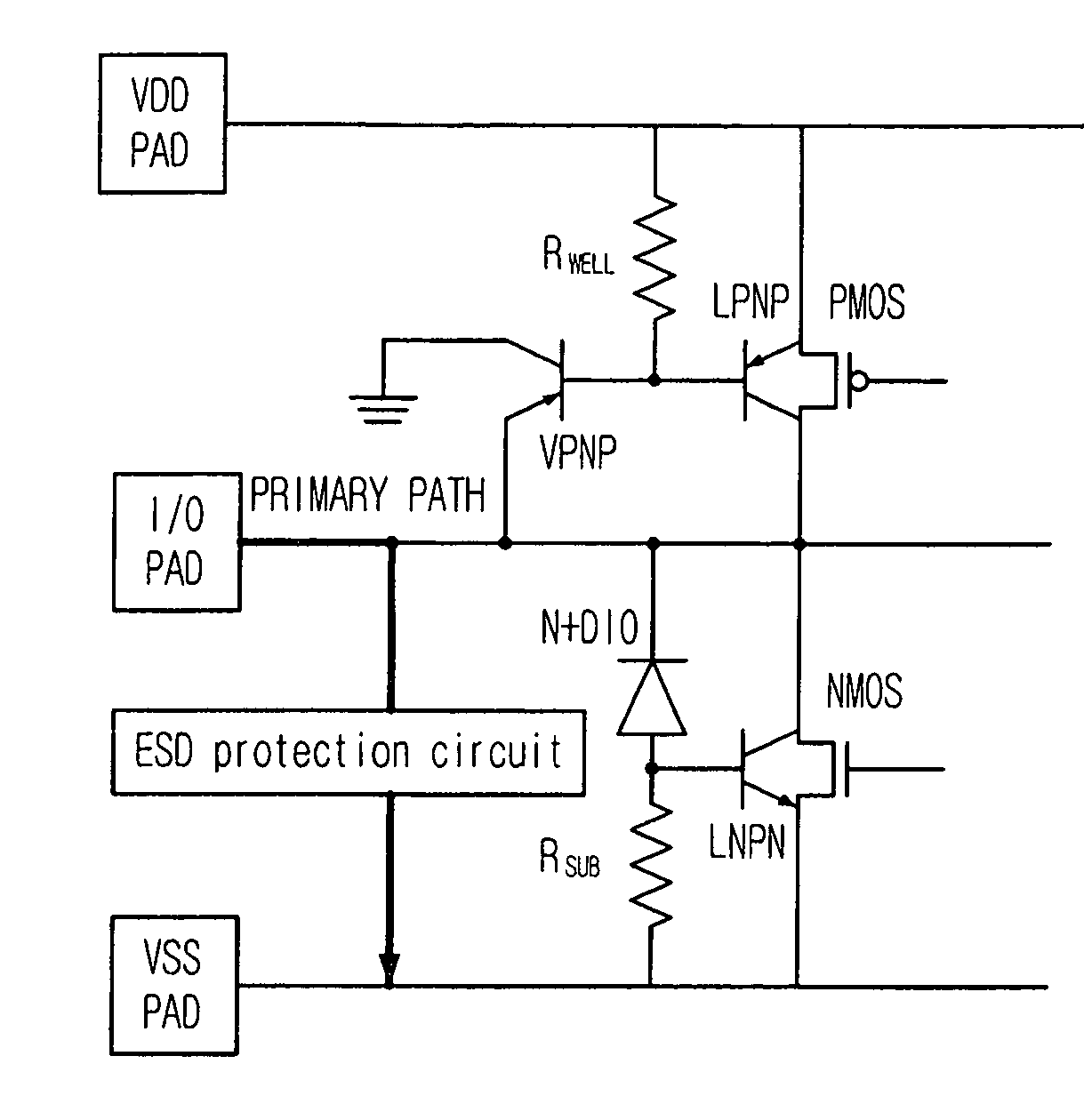
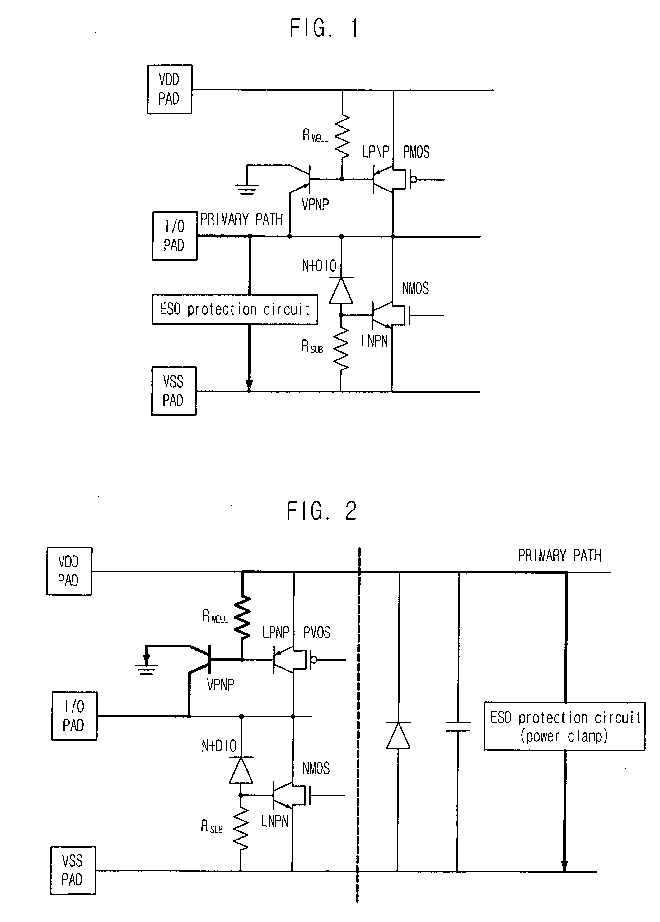
ESD protection circuit
a protection circuit and electrostatic discharge technology, applied in the field of semiconductor devices, can solve the problems of difficult to expect that a stable and efficient esd protection performance will be acquired, the layout area in which an individual esd protection circuit can be installed at each i/o pad cannot be secured, and the relative difficulty of acquiring a stable esd protection characteristic compared with the dpbesd protection circui
- Summary
- Abstract
- Description
- Claims
- Application Information
AI Technical Summary
Benefits of technology
Problems solved by technology
Method used
Image

Examples
first embodiment
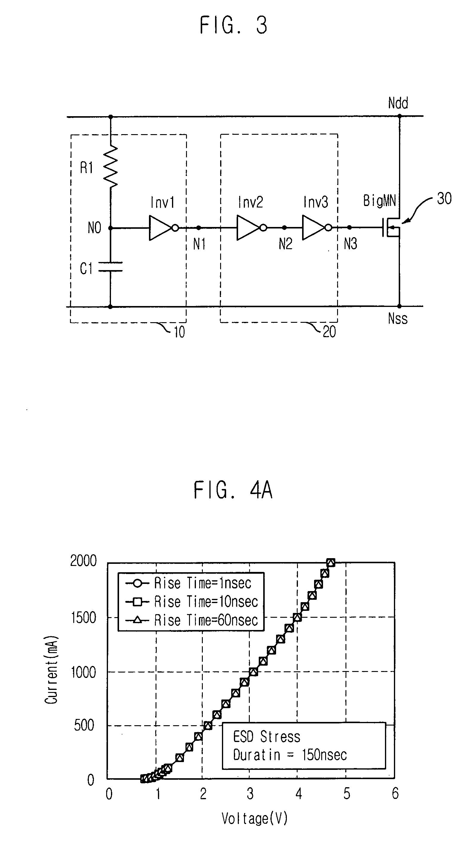
[0045]FIG. 6 illustrates a circuit diagram for describing a configuration and its operation principle of an RBNB ESD protection circuit in accordance with the present invention, wherein it is called 1RC3Inv_LPC ESD protection circuit and LPC means “Leakage Prevention Capacitor”.
[0046] Referring to FIG. 6, the RBNB ESD protection circuit fundamentally cuts off a leakage current path by additionally installing a capacitor Clp between Ndd and source of a PMOS transistor PM (see FIG. 7) of an inverter Inv1 of the 1RC3Inv_std protection circuit.
[0047] That is, in order to cut off a leakage current flowing through a PMOS transistor PM and an NMOS transistor NM of an inverter Inv1 constituting a rising time detector 110 that detects a rising time of an ESD stress current when a noise varied at a speed faster than a time constant of an RC filter is applied between Ndd and Nss lines, the RBNB ESD protection circuit in accordance with the first embodiment of the invention connects a capacito...
second embodiment
[0061] In order to help understand a configuration of an RBNB ESD protection circuit according to the invention shown in FIG. 10, a configuration of a conventional 2RC2Inv_std ESD protection circuit is shown in FIG. 11.
[0062] As depicted in FIG. 11, the conventional 2RC2Inv_std ESD protection circuit is another type of the RBNB ESD protection circuit. Unlike the 1RC3Inv_std ESD protection circuit shown in FIG. 3, the conventional 2RC2Inv_std ESD protection circuit is comprised of two resistors R1 and R2, two capacitors C1 and C2, two inverters Inv1 and Inv2, and one NMOS transistor NM as a boosting circuit for operating a big MOS transistor BigMN of a power clamp 330. That is, a rising time detector 310 is composed of an RC filter R1 and C1 and an inverter Inv1, and a pre-driver 320 is composed of a resistor R2 coupled between Ndd and the node N2, a capacitor C2 coupled in parallel to the resistor R2, a transistor NM that operates in response to an output of the inverter Inv1 and co...
PUM
 Abstract
Description
Claims
Application Information