Oled devices with dinuclear copper compounds

a technology of dinuclear copper and oled devices, which is applied in the direction of discharge tube luminescnet screens, natural mineral layered products, etc., can solve the problems of large loss of efficiency, material emissivity when irradiated by visible light, and performance limitations that are not suitable for many desirable applications

Active Publication Date: 2007-05-17
UNIVERSITY OF ROCHESTER +1
View PDF4 Cites 568 Cited by
  • Summary
  • Abstract
  • Description
  • Claims
  • Application Information

AI Technical Summary

Problems solved by technology

While organic electroluminescent (EL) devices have been known for over two decades, their performance limitations have represented a barrier to many desirable applications.
However, it is generally believed that only 25% of the excitons created in an EL device are singlet excitons.
This results in a large loss in efficiency since 75% of the excitons are not used in the light emission process.
In selecting materials for use in an OLED device, in particular as a phosphorescent emitter, it is not sufficient that the material is emissive when irradiated by visible light.
In addition, iridium and platinum are particularly expensive metals.

Method used


Image

  • Oled devices with dinuclear copper compounds
  • Oled devices with dinuclear copper compounds
  • Oled devices with dinuclear copper compounds

Examples


example 1

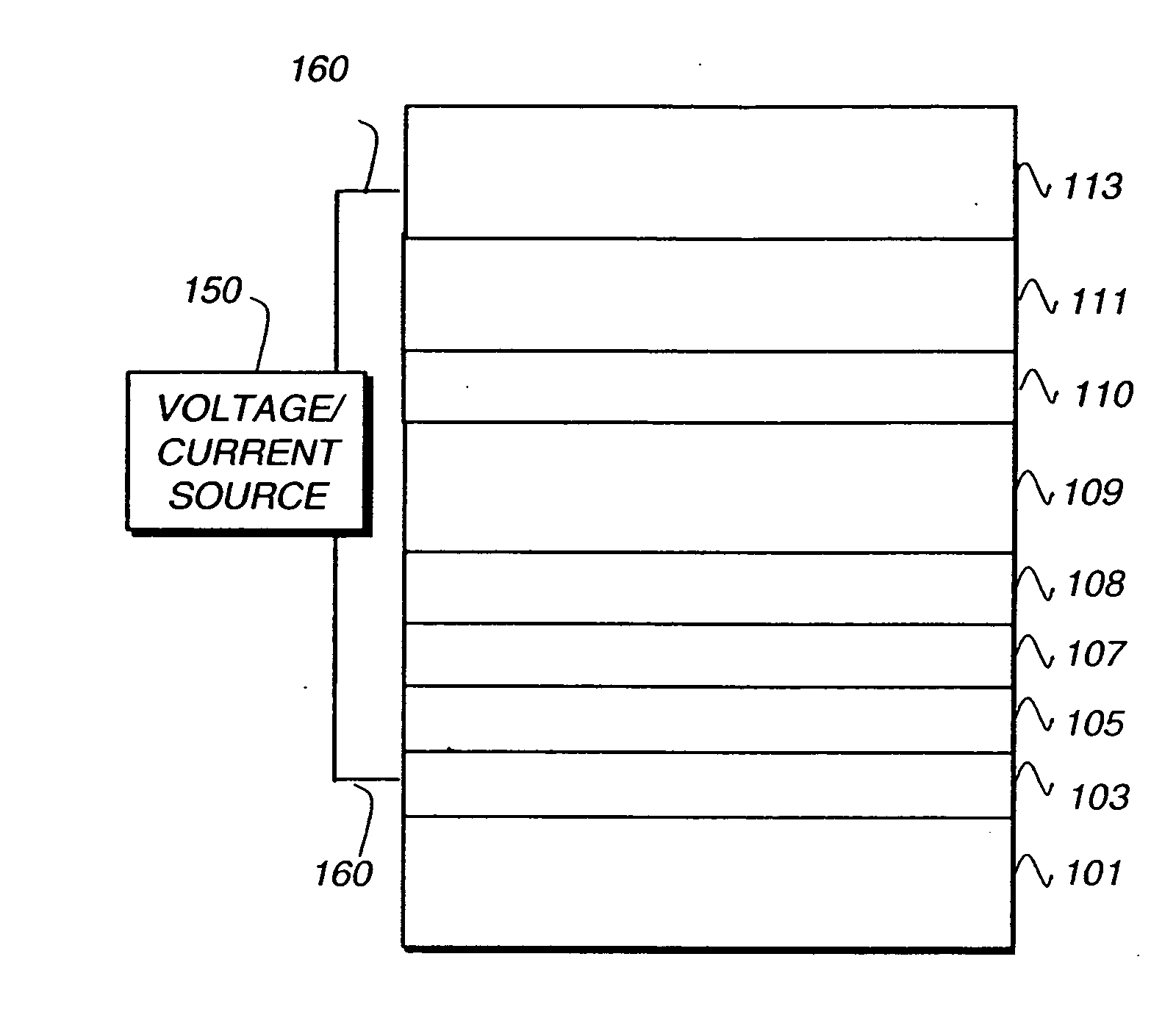
[0284] An EL device (Sample 1) satisfying the requirements of the invention was constructed in the following manner:

[0285] 1. A glass substrate coated with an 85 nm layer of indium-tin oxide (ITO) as the anode was sequentially ultrasonicated in a commercial detergent, rinsed in deionized water, degreased in toluene vapor and exposed to oxygen plasma for about 1 min.

[0286] 2. Over the ITO was deposited a 1 nm fluorocarbon (CFx) hole-injecting layer (HIL) by plasma-assisted deposition of CHF3.

[0287] 3. A hole-transporting layer (HTL)of N,N′-di-1-naphthyl-N,N′-diphenyl-4,4′-diaminobiphenyl (NPB) having a thickness of 75 nm was then evaporated from a tantalum boat.

[0288] 4. A 35 nm light-emitting layer (LEL) of 4,4′-N,N′-dicarbazole-biphenyl (CBP) and Inv-1 (1 wt %) were then deposited onto the hole-transporting layer. These materials were also evaporated from tantalum boats.

[0289] 5. A hole-blocking layer of bis(2-methyl-quinolinolato)(2,4,6-triphenylphenolato)aluminum(III) (Balq)...

example 2

[0294] An EL device (Sample 7) satisfying the requirements of the invention was constructed in the following manner:

[0295] 1. A glass substrate coated with an 85 nm layer of indium-tin oxide (ITO) as the anode was sequentially ultrasonicated in a commercial detergent, rinsed in deionized water, degreased in toluene vapor and exposed to oxygen plasma for about 1 min.

[0296] 2. Over the ITO was deposited a 1 nm fluorocarbon (CFx) hole-injecting layer (HIL) by plasma-assisted deposition of CHF3.

[0297] 3. A hole-transporting layer (HTL) of N,N′-di-1-naphthyl-N,N′-diphenyl-4,4′-diaminobiphenyl (NPB) having a thickness of 95 nm was then evaporated from a tantalum boat.

[0298] 4. A 35 nm light-emitting layer (LEL) of 9,9′-(1,3-phenylene)bis-9H-carbazole (mCP) and Inv-1 (8 wt %) were then deposited onto the hole-transporting layer. These materials were also evaporated from tantalum boats.

[0299] 5. A hole-blocking layer of bis(2-methyl-quinolinolato)(2,4,6-triphenylphenolato)aluminum(III)...

example 3

[0303] An EL device (Sample 8) satisfying the requirements of the invention was constructed in the following manner:

[0304] 1. A glass substrate coated with an 85 nm layer of indium-tin oxide (ITO) as the anode was sequentially ultrasonicated in a commercial detergent, rinsed in deionized water, degreased in toluene vapor and exposed to oxygen plasma for about 1 min.

[0305] 2. Over the ITO was deposited a 1 nm fluorocarbon (CFx) hole-injecting layer (HIL) by plasma-assisted deposition of CHF3.

[0306] 3. A hole-transporting layer (HTL) of N,N′-di-1-naphthyl-N,N′-diphenyl-4,4′-diaminobiphenyl (NPB) having a thickness of 95 nm was then evaporated from a tantalum boat.

[0307] 4. A 35 nm light-emitting layer (LEL) of 4-(9H-carbazol-9-yl)-N,N-bis[4-(9H-carbazol-9-yl)phenyl]-benzenamine (TCTA) and Inv-1 (8 wt %) were then deposited onto the hole-transporting layer. These materials were also evaporated from tantalum boats.

[0308] 5. A hole-blocking layer of bis(2-methyl-quinolinolato)(2,4,6...


PUM

PropertyMeasurementUnit
wt %aaaaaaaaaa
triplet energyaaaaaaaaaa
LUMO energy levelaaaaaaaaaa

Abstract

An OLED device comprises an anode, a cathode and therebetween a light emitting layer containing a compound represented by Formula I below:
wherein: each A is independently selected from N and P; each E is independently selected from N, P, and As;
each Z is a radical independently selected from
each R is an independently selected substituent; and each R′ is independently selected from H and a substituent; provided that two substituent groups can join to form a ring.

Description

FIELD OF INVENTION [0001] This invention relates to organic electroluminescent (EL) devices employing certain copper based light emitting compounds. BACKGROUND OF THE INVENTION [0002] While organic electroluminescent (EL) devices have been known for over two decades, their performance limitations have represented a barrier to many desirable applications. In simplest form, an organic EL device is comprised of an anode for hole injection, a cathode for electron injection, and an organic medium sandwiched between these electrodes to support charge recombination that yields emission of light. These devices are also commonly referred to as organic light-emitting diodes, or OLEDs. Representative of earlier organic EL devices are Gurnee et al. U.S. Pat. No. 3,172,862, issued Mar. 9, 1965; Gurnee U.S. Pat. No. 3,173,050, issued Mar. 9, 1965; Dresner, “Double Injection Electroluminescence in Anthracene”, RCA Review, Vol. 30, pp. 322-334, 1969; and Dresner U.S. Pat. No. 3,710,167, issued Jan....

Claims


Application Information

Patent Timeline
Patent Type & Authority Applications(United States)
IPC IPC(8): H01L51/54
CPCC09K11/06C09K2211/1014C09K2211/188H01L51/009H01L51/5016H01L51/5096H05B33/14Y10S428/917H10K85/361H10K50/18H10K50/11H10K2101/10
Inventor DEATON, JOSEPH C.EISENBERG, RICHARD S.
Owner UNIVERSITY OF ROCHESTER
Why Eureka
Try Eureka