Metal-free silicon-molecule-nanotube testbed and memory device

a silicon-molecule, memory device technology, applied in the field ofmolecular electronics, can solve the problems of persistent problems in ultrathin sandwich structure, affecting the conduction through molecular junction, and devices that are not molecular-monolayer-based, and achieve the effect of no hysteresis

Inactive Publication Date: 2007-05-17
RICE UNIV
View PDF3 Cites 4 Cited by
  • Summary
  • Abstract
  • Description
  • Claims
  • Application Information

AI Technical Summary

Benefits of technology

[0009] In view of the foregoing considerations, the present invention is related to a method for testing molecules with a testbed structure containing two oxide-free non-metallic electrodes in order to eliminate the possibility of metal-filament formation and to reveal the molecular effects. Then, with u-conjugated molecular structures, a hysteresis can be observed that can serve as a molecular electronic memory.
[0010] In one aspect, the present invention is directed generally to a method of making reliable electrical contacts to molecules for the purposes of creating a testbed for testing and utilizing, the electronic properties of the molecules. In one embodiment, the invention features the deposition of carbon nanotubes atop a molecular layer to form the top electrical contact (electrode), instead of the prior art method of forming the top contact via physical vapor deposition (PVD) of a metal or deposition of metal nanoparticles. By practicing the present invention, molecules can be reliably connected to the bottom and top electrodes, and their electronic behavior can be determined by the corresponding testing.

Problems solved by technology

However, there are perceived uncertainties about the switching mechanisms, the local environment, as well as temperature, which can potentially affect the conduction through molecular junctions.
Whereas organic films deposited from solution or by sublimation have been used in organic field-effect transistors with some success, such devices are not molecular-monolayer based.
Several persistent problems arise in these ultrathin sandwich structures.
First, as the top electrode is vapor-deposited onto the self-assembled monolayer, energetic metal atoms can degrade the molecules.
Second, the metal

Method used


Image

  • Metal-free silicon-molecule-nanotube testbed and memory device
  • Metal-free silicon-molecule-nanotube testbed and memory device
  • Metal-free silicon-molecule-nanotube testbed and memory device

Examples


Embodiment Construction

[0025] In the following description, specific parametric details are set forth, including specific quantities, sizes, materials, properties, and the like, so as to provide a thorough understanding of the present invention. However, it will be readily apparent to those of ordinary skill in the art that the present invention may be practiced while deviating to varying extents from specifically detailed parameters. In many cases, details concerning certain features and parameters of the invention have been omitted, inasmuch as such details are not believed to be necessary to obtain a complete understanding of the present invention and are within the skills of persons of ordinary skill in the relevant art.

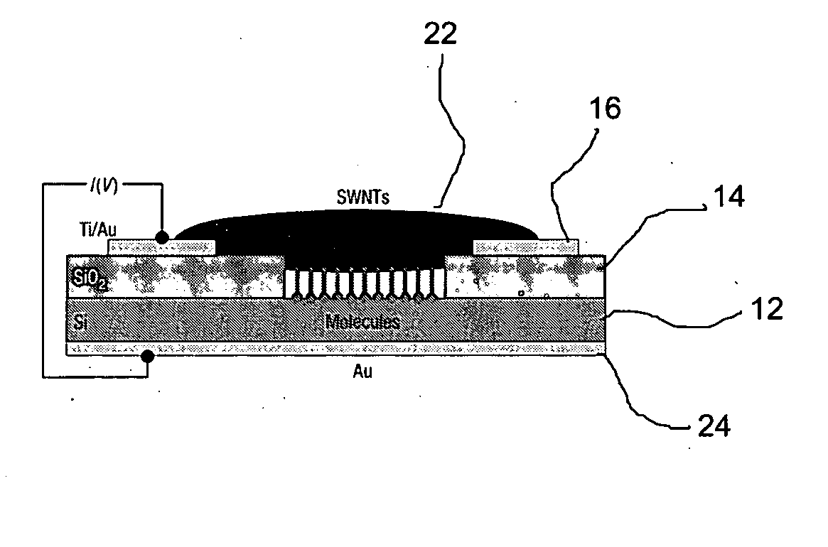
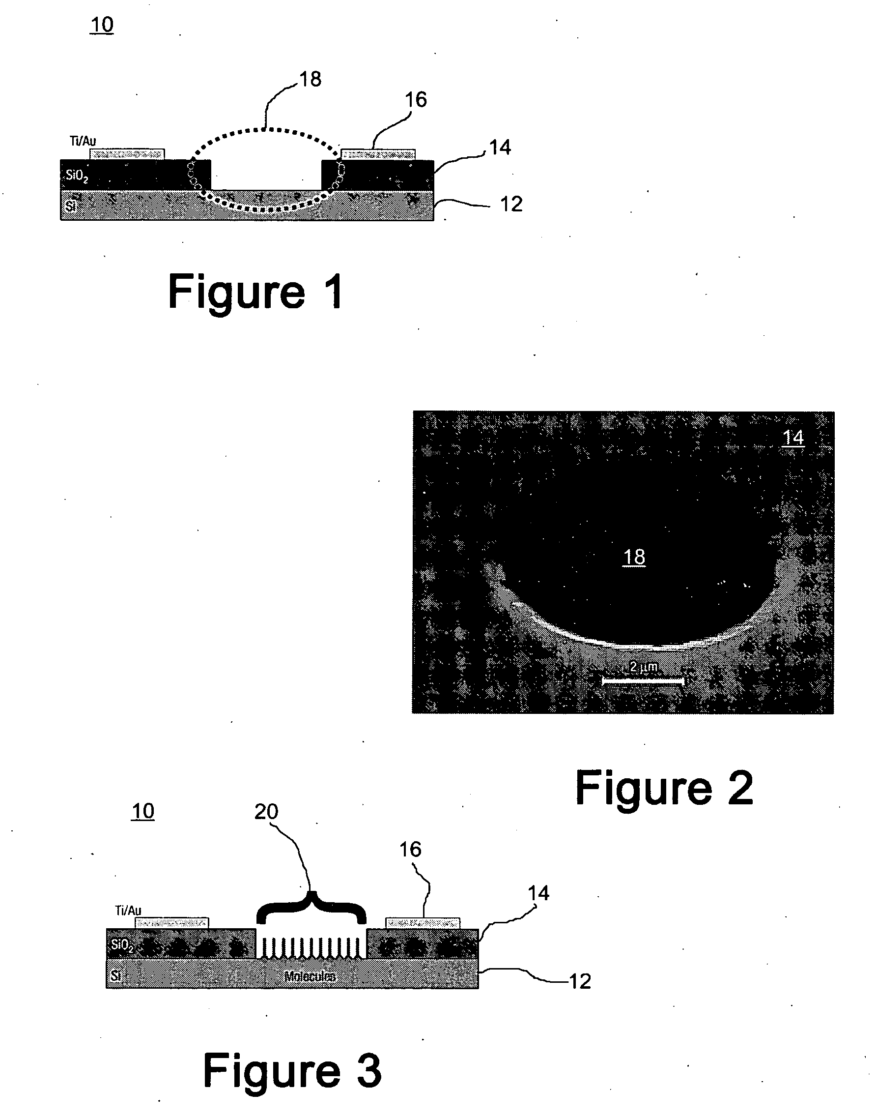
[0026] Referring to FIG. 1, there is shown the starting lithographically defined structure of a silicon-molecule-SWNT device 10 in accordance with one embodiment of the invention. As shown in FIG. 1, structure 10 comprises a silicon substrate 12 upon which is formed an oxide layer 14 ...


PUM


Abstract

Work from several laboratories has shown that metal nanofilaments cause problems in some molecular electronics testbeds. A new testbed for exploring the electrical properties of single molecules has been developed to eliminate the possibility of metal nanofilament formation and to ensure that molecular effects are measured. This metal-free system uses single-crystal silicon and single-walled carbon nanotubes as electrodes for the molecular monolayer. A direct Si-arylcarbon grafting method is used. Use of this structure with π-conjugated organic molecules results in a hysteresis loop with current-voltage measurements that are useful for an electronic memory device. The memory is non-volatile for more than 3 days, non-destructive for more than 1,000 reading operations and capable of more than 1,000 write-erase cycles before device breakdown. Devices without π-conjugated molecules (Si—H surface only) or with long-chain alkyl-bearing molecules produced no hysteresis, indicating that the observed memory effect is molecularly relevant.

Description

RELATED APPLICATION DATA [0001] Pursuant to 35 U.S.C. § 119, this application claims the priority of prior provisional application Ser. No. 60 / 645,814, filed on Jan. 21, 2005, which application being hereby incorporated by reference herein in its entirety.STATEMENT REGARDING FEDERALLY SPONSORED RESEARCH OR DEVELOPMENT [0002] The research and development related to this invention was funded at least in part by the U.S. Defense Advanced Research Projects Agency through the Air Force Office of Scientific Research, Grant No. ______.FIELD OF THE INVENTION [0003] The present invention is directed generally to the field of molecular electronics, and more particularly to metal-free silicon-molecule-nanotube systems. BACKGROUND OF THE INVENTION [0004] Speculation that silicon-based semiconductor manufacturing processes will encounter a miniaturization limit has led to a large research effort in molecular electronics, where molecular monolayers are used as active switching components. In the ...

Claims


Application Information

Patent Timeline
IPC IPC(8): H01L21/20
CPCB82Y10/00B82Y30/00G11C13/0014G11C13/02G11C13/025H01L27/283H01L51/0048H01L51/005H01L51/0052H01L51/0595H10K19/10H10K85/60H10K85/221H10K85/615H10K10/701
Inventor TOUR, JAMES M.HE, JIANLICHEN, BOFLATT, AUSTEN K.STEPHENSON, JASON J.DOYLE, CONDELL D.
Owner RICE UNIV
Why Eureka
Try Eureka