

Integrated electroless deposition system
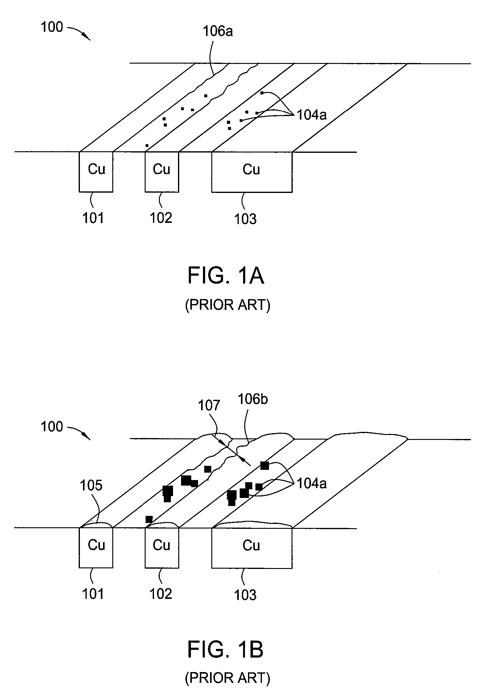
a technology of electroless deposition and integrated deposition, which is applied in the direction of liquid/solution decomposition, electrolysis components, coatings, etc., can solve the problems of copper leaking into neighboring layers, copper suffers by diffusing into neighboring layers, and dielectric layers to become conductive, etc., to achieve high aspect ratio and low aspect ratio
- Summary
- Abstract
- Description
- Claims
- Application Information
AI Technical Summary
Problems solved by technology
Method used
Image

Examples
Embodiment Construction
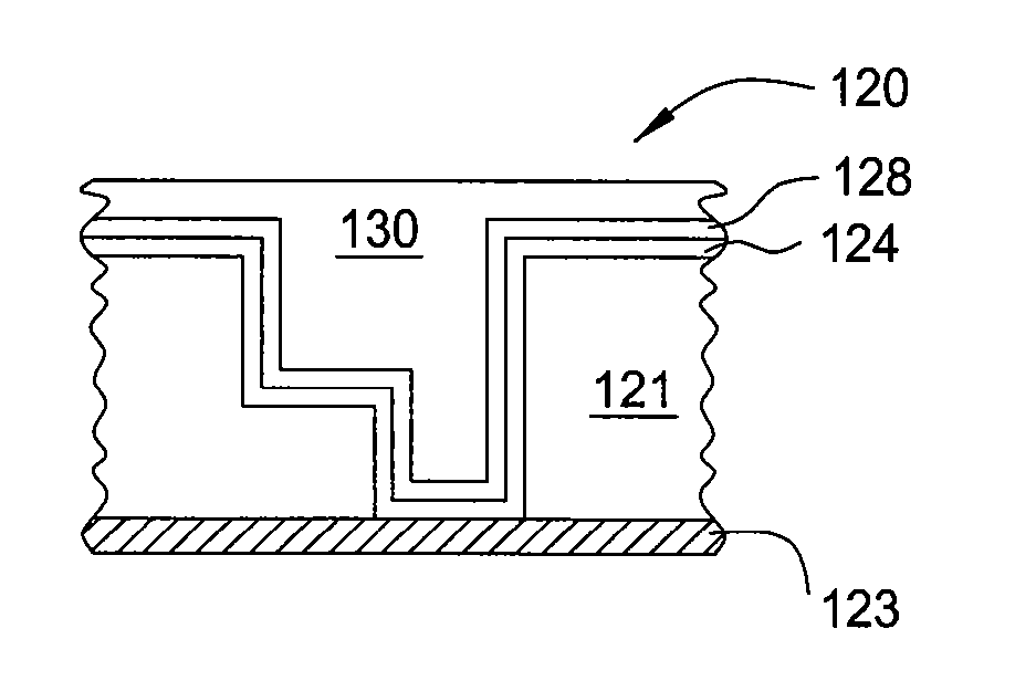
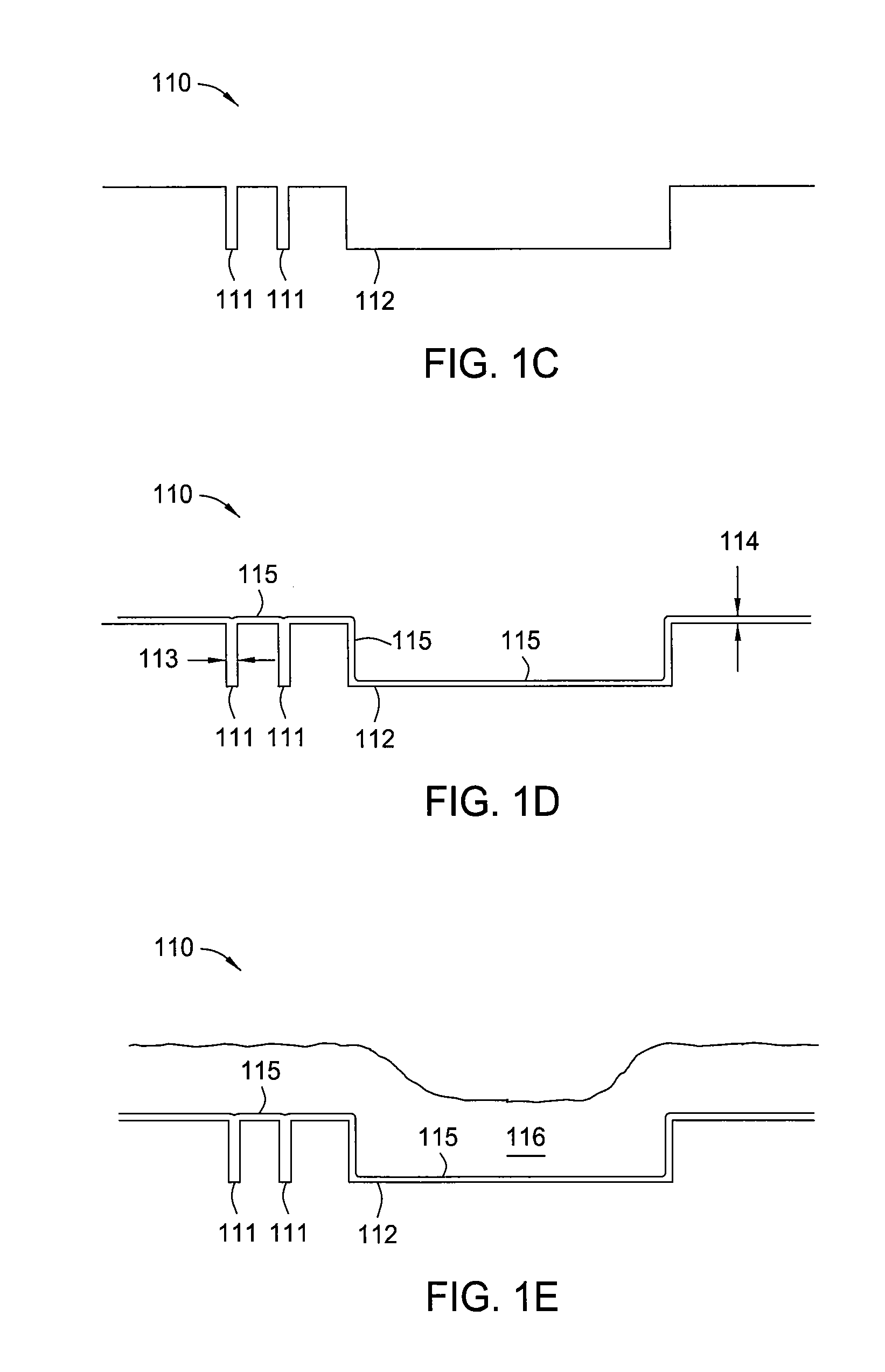
[0067] Embodiments of the invention generally provide methods of depositing materials onto semiconductor substrates by using one or more electroless, ECP, CVD and / or ALD processing chambers. More particularly, embodiments of the invention allow formation of capping layers with low defects and low oxidation of interconnect features, deposition of a barrier layer on substrates, deposition and / or repair of seed layers on substrates, electroless fill of interconnect features, and sequential filling of high and low aspect ratio interconnect features on a substrate, using electroless and ECP processes. Other embodiments of the invention allow the removal of native oxides and other contaminants on exposed contacts at the bottom of high aspect ratio features and the subsequent deposition of cobalt and / or nickel to fill such contacts. In one aspect, nickel silicide is formed after an oxide cleaning step and before a cobalt fill step to prevent further silicidation of diffused cobalt into sil...
PUM
| Property | Measurement | Unit |
|---|---|---|
| temperature | aaaaa | aaaaa |
| temperature | aaaaa | aaaaa |
| aspect ratio | aaaaa | aaaaa |
Abstract
Description
Claims
Application Information