
Photoelectric conversion device

a conversion device and photoelectric technology, applied in the direction of semiconductor devices, diodes, electrical apparatus, etc., can solve the problems of deterioration of operation characteristics, and achieve the effect of improving reliability and reducing character deterioration

Inactive Publication Date: 2007-05-24
SEMICON ENERGY LAB CO LTD
View PDF18 Cites 59 Cited by
  • Summary
  • Abstract
  • Description
  • Claims
  • Application Information

AI Technical Summary

Benefits of technology

The present invention relates to a photoelectric conversion device used in electronic devices such as cell phones. The invention improves the reliability of the device by reducing deterioration caused by stress and improving the sensitivity of the device. This is achieved by improving the cross-sectional shape of the electrodes in contact with the photoelectric conversion layer. By making the cross-sectional shape of the electrodes a taper shape, the device can improve step coverage and relieve electric or physical stress. Additionally, the invention includes a protective film with a taper shape to improve step coverage and relieve stress. The protective film can selectively transmit light of a specific wavelength band and can be made of a light transmitting resin or a photosensitive material. The invention also includes a thin film transistor for holding the electrodes and the photoelectric conversion layer. The substrate can be flexible and the device can be applied to various electronic devices. Overall, the invention improves the reliability of the photoelectric conversion device and enhances its performance.

Problems solved by technology

However, a photoelectric conversion device that is formed by stacking a thin film, such as an amorphous silicon photodiode or a thin film transistor, has a problem that an operation characteristic is deteriorated by adding a stress due to electric or physical operation.

Method used


Image

  • Photoelectric conversion device
  • Photoelectric conversion device
  • Photoelectric conversion device

Examples


embodiment 1

[0046] In this embodiment, one example of a photoelectric conversion device using a thin film transistor and a photodiode will be explained.

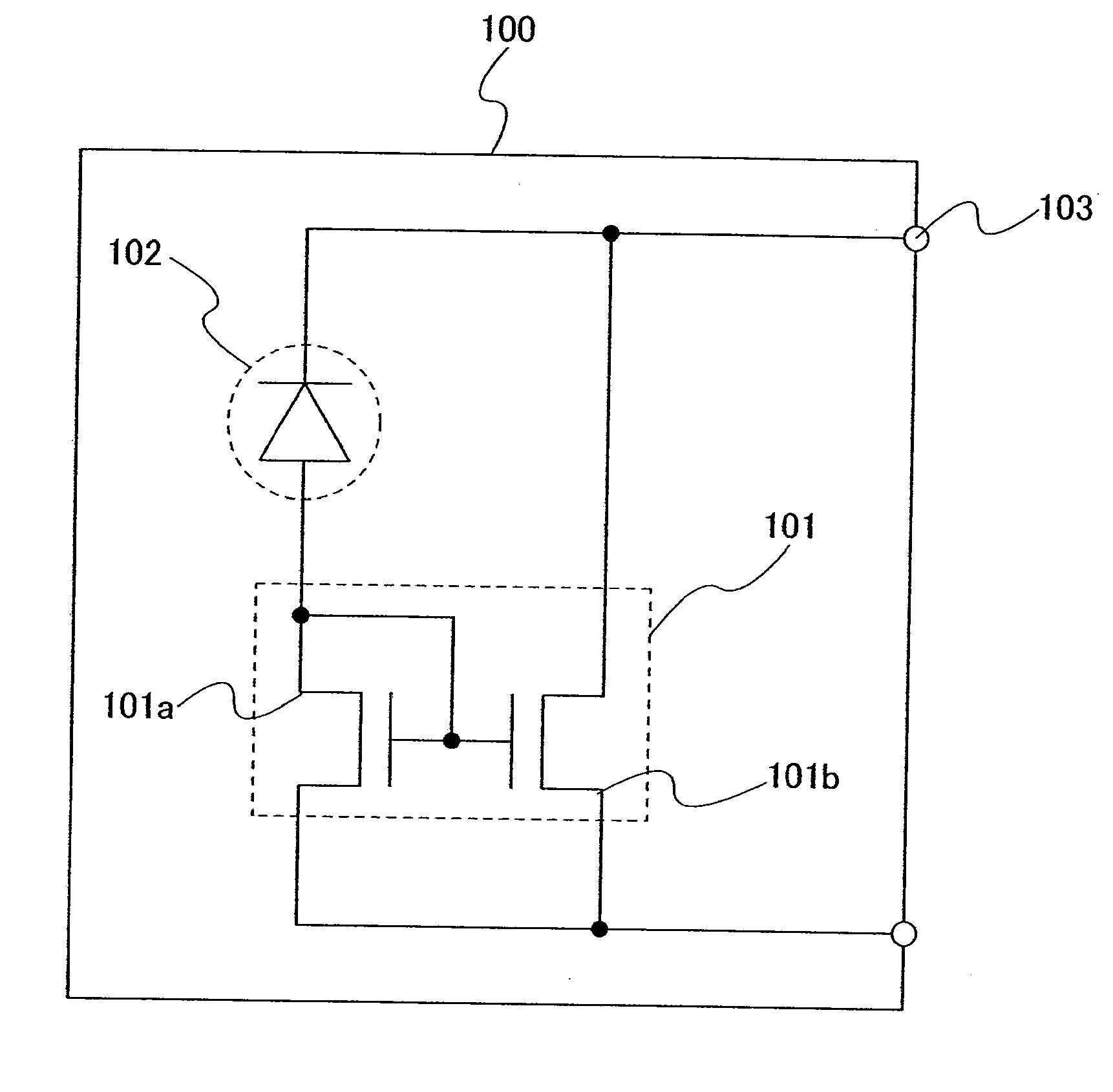
[0047] In a photoelectric conversion device shown in this embodiment, a photodiode and an amplifier circuit that is formed by a thin film transistor are formed in an integrated manner over a same substrate. FIG. 1 shows one example of a configuration as a circuit diagram. This photoelectric conversion device 100 is provided with an amplifier circuit 101 that amplifies output of a photodiode 102. Various circuit configurations can be applied to the amplifier circuit 101. In this embodiment, a current mirror circuit is formed by a thin film transistor 101a and a thin film transistor 101b. Source terminals of the thin film transistors 101a and 101b are each connected to an external power supply GND. A drain terminal of the thin film transistor 101b is connected to an output terminal 103. The photodiode 102 may be provided with a pn junction, a pin...

embodiment 2

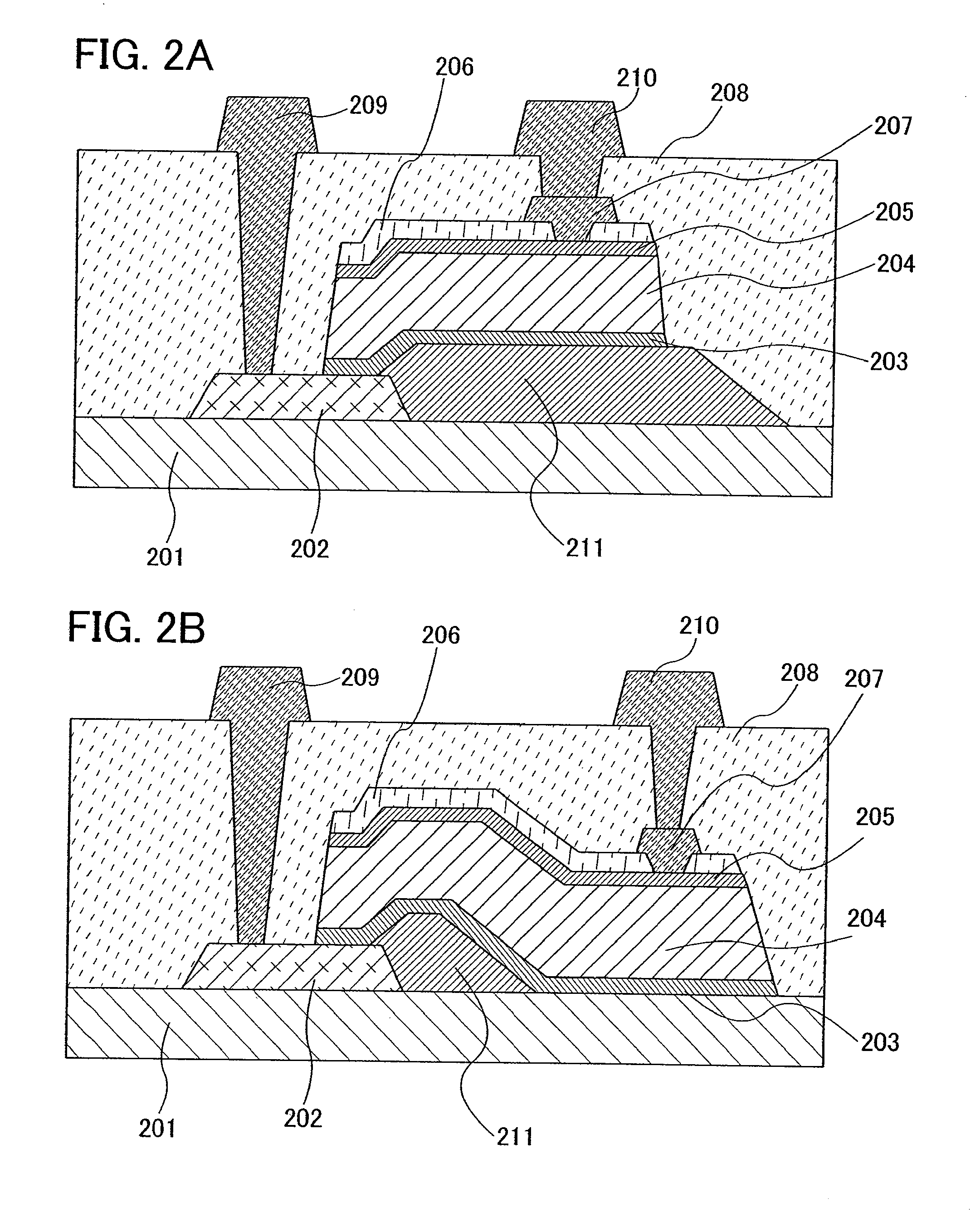
[0065] In this embodiment, in order to improve reliability of a photoelectric conversion device, an example of manufacturing a photoelectric conversion layer by protecting an edge portion of an electrode by a protective film after forming a thin film transistor will be explained with reference to FIGS. 4A to 4D, and FIGS. 5A to 5C. It is to be noted that the same portion with that in Embodiment 1 is denoted by the same reference numeral, and the photoelectric conversion layer may be manufactured based on the manufacturing step described in Embodiment 1.

[0066] In FIG. 4A, the electrode 403 is etched to form the electrode 404. At this time, a shape of an edge portion of the electrode 404 may not be a taper shape; however, by making the edge portion have a taper shape, coverage of a protective film 412 formed afterwards can be improved.

[0067] Next, the protective film 412 is formed from polyimide (refer to FIG. 5A). In this embodiment, the protective film is formed so as to transmit ...

embodiment 3

[0071] In this embodiment, in order to improve reliability of a photoelectric conversion device, in a case where a photoelectric conversion layer is manufactured by protecting an edge portion of an electrode by a protective film after forming a thin film transistor, an example of changing a pattern of the protective film will be explained with reference to FIG. 5C and FIG. 6A. It is to be noted that the same portion with that in Embodiment 2 is denoted by the same reference numeral, and the photoelectric conversion layer may be manufactured based on the manufacturing step described in Embodiment 2.

[0072] The protective film in FIG. 5C can be formed only on the periphery of the electrode 404 (refer to FIG. 6A).

[0073] By utilizing this embodiment, the photoelectric conversion layer can be used even when the protective film has no light transmitting property. In addition, light transmittance is increased, and then, efficiency of photoelectric conversion can be enhanced. Moreover, ope...


PUM


Abstract

A photoelectric conversion device provided with a photoelectric conversion layer between a first electrode and a second electrode is formed. The first electrode is partially in contact with the photoelectric conversion layer, and a cross-sectional shape of the first electrode in the contact portion is a taper shape. In this case, part of a first semiconductor layer with one conductivity type is in contact with the first electrode. A planer shape in an edge portion of the first electrode is preferably nonangular, that is, a shape in which edges are planed or a curved shape. By such a structure, concentration of an electric field and concentration of a stress can be suppressed, whereby characteristic deterioration of the photoelectric conversion device can be reduced.

Description

TECHNICAL FIELD [0001] The present invention relates to a photoelectric conversion device that outputs an electric signal depending on intensity of light that is received. BACKGROUND ART [0002] As a photoelectric conversion device used for detecting an electromagnetic wave, one having sensitivity from UV light to infrared light is also called a light sensor in general. Above all, one having sensitivity in a visible light ray region with a wave length of 400 to 700 nm is called a visible light sensor, which is variously used for equipment that needs illuminance adjustment or on-off control depending on living environment. [0003] A light sensor device is known, in which, with the use of an amorphous silicon photodiode that is used as such a light sensor that has sensitivity in a visible light ray region, the amorphous silicon photodiode and an amplifier including a thin film transistor are formed in an integrated manner (for example, refer to Patent Document 1: Japanese Published Pate...

Claims


Application Information

Patent Timeline
Patent Type & Authority Applications(United States)
IPC IPC(8): H01L31/00
CPCH01L27/14643H01L27/14692H01L27/14636H01L31/03762H01L27/14609H01L31/022408H01L27/14H01L31/10
Inventor ARAO, TATSUYAKUSUMOTO, NAOTOYAMADA, DAIKITAKAHASHI, HIDEKAZUNISHI, KAZUOSUGAWARA, YUUSUKETAKAHASHI, HIRONOBUFUKAI, SHUJI
Owner SEMICON ENERGY LAB CO LTD
Features
  • Generate Ideas
  • Intellectual Property
  • Life Sciences
  • Materials
  • Tech Scout
  • Unparalleled Data Quality
  • Higher Quality Content
  • 60% Fewer Hallucinations
Learn More