Semiconductor device and method of fabricating the same

a semiconductor laser diode and semiconductor technology, applied in the direction of semiconductor lasers, crystal growth process, polycrystalline material growth, etc., can solve the problem of reducing the luminous efficiency of nitride semiconductor laser diodes, and achieve the effect of improving the surface morphology characteristi

Inactive Publication Date: 2007-05-24
SAMSUNG ELECTRONICS CO LTD
View PDF6 Cites 34 Cited by
  • Summary
  • Abstract
  • Description
  • Claims
  • Application Information

AI Technical Summary

Benefits of technology

[0015] According to exemplary embodiments of the present disclosure, a semiconductor device having an improved surface morphology characteristic can be obtained.

Problems solved by technology

Thus, in nitride semiconductor laser diodes, the probability of combining electrons with holes can be reduced by the effect of an internal electric field formed by polarization of the c-plane, which lowers the luminous efficiency of the nitride semiconductor laser diodes.

Method used


Image

  • Semiconductor device and method of fabricating the same
  • Semiconductor device and method of fabricating the same
  • Semiconductor device and method of fabricating the same

Examples


Embodiment Construction

[0027] The present invention will now be described more fully with reference to the accompanying drawings, in which exemplary embodiments of the invention are shown. In the drawings, the thicknesses of layers and regions are exaggerated for clarity.

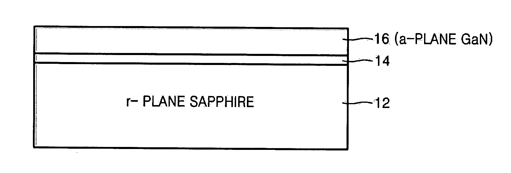
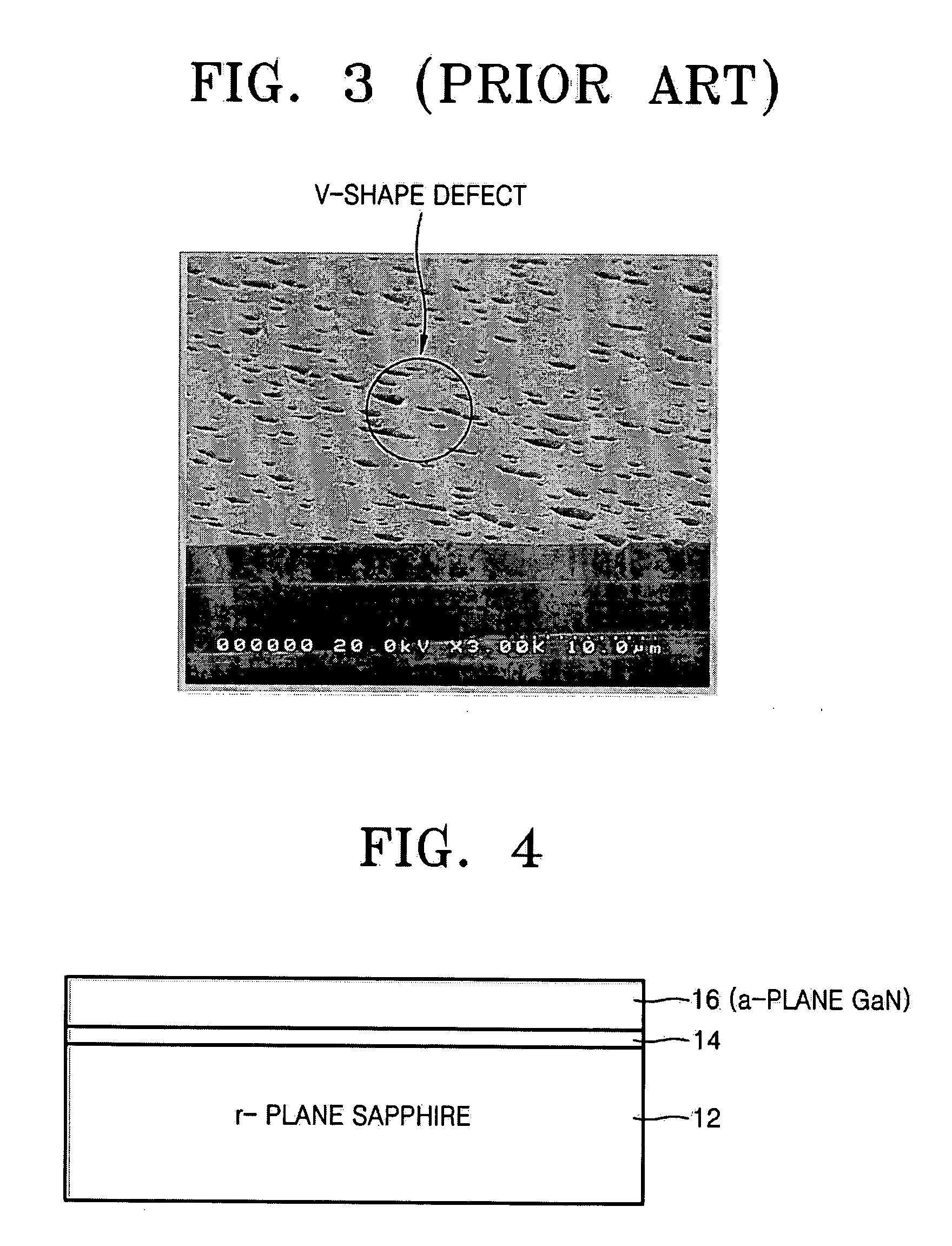
[0028]FIG. 4 is a cross-sectional view of a semiconductor device according to an embodiment of the present disclosure, and FIGS. 5 and 6 are respectively a cross-section SEM photo and a surface SEM photo of the semiconductor device illustrated in FIG. 4.

[0029] Referring to FIGS. 4 through 6, the semiconductor device according to an embodiment of the present disclosure includes an AlxGa(1-x)N(0≦×14 and a first a-plane GaN layer 16, which are sequentially stacked on an r-plane sapphire substrate 12. The semiconductor device illustrated in FIG. 4 may be used as a semiconductor substrate for fabricating a GaN-based device.

[0030] The buffer layer 14 may be epitaxially grown to a thickness in the range of 100-20000 Å in a gas atmosphere cont...


PUM

PropertyMeasurementUnit
temperatureaaaaaaaaaa
pressureaaaaaaaaaa

Abstract

Provided are semiconductor devices having improved surface morphology characteristics, and a method of fabricating the same. The semiconductor device includes: an r-plane sapphire substrate; an AlxGa(1-x)N(0≦×<1) buffer layer epitaxially grown on the r-plane sapphire substrate to a thickness in the range of 100-20000 Å in a gas atmosphere containing nitrogen (N2) and at a temperature of 900-1100° C.; and a first a-plane GaN layer formed on the buffer layer.

Description

CROSS-REFERENCE TO RELATED PATENT APPLICATIONS [0001] Priority is claimed to Korean Patent Application Nos. 10-2005-0110882 and 10-2006-0102046, filed on Nov. 18, 2005 and Oct. 19, 2006, in the Korean Intellectual Property Office, the disclosures of which are incorporated herein in its entirety by reference. BACKGROUND OF THE DISCLOSURE [0002] 1. Field of the Disclosure [0003] The present disclosure relates to a GaN semiconductor device, and more particularly, to a semiconductor device having improved surface morphology characteristics, and a method of fabricating the same. [0004] 2. Description of the Related Art [0005] Conventional GaN-based devices, for example, nitride semiconductor laser diodes, are implemented on a c-plane GaN substrate. However, the c-plane of GaN crystal is well-known as a polar plane. Thus, in nitride semiconductor laser diodes, the probability of combining electrons with holes can be reduced by the effect of an internal electric field formed by polarizatio...

Claims


Application Information

Patent Timeline
Patent Type & Authority Applications(United States)
IPC IPC(8): H01L33/00H01S5/343
CPCB82Y20/00C30B25/02C30B29/403C30B29/406H01L21/0242H01L21/02433H01L21/02458H01L21/02516H01L21/0254H01L21/02609H01L21/0262H01S5/0213H01S5/3202H01S5/34333H01S2301/173H01S5/04257H01S5/32025
Inventor PAEK, HO-SUNSAKONG, TANSON, JOONG-KONLEE, SUNG-NAM
Owner SAMSUNG ELECTRONICS CO LTD
Why Eureka
Try Eureka