Semiconductor device, method of manufacturing the same and power converter

a technology of semiconductor devices and semiconductor layers, which is applied in the direction of efficient power electronics conversion, climate sustainability, semiconductor devices, etc., can solve the problems of deterioration of device characteristics, deterioration of surface morphology, and reduction of the crystallinity of the semiconductor layer formed, so as to improve the surface morphology of the p-type semiconductor region and improve the device characteristics of the semiconductor devi

Active Publication Date: 2017-03-16
TOYODA GOSEI CO LTD
View PDF5 Cites 10 Cited by
  • Summary
  • Abstract
  • Description
  • Claims
  • Application Information

AI Technical Summary

Benefits of technology

[0009](1) According to one aspect of the invention, there is provided a method of manufacturing a semiconductor device. This method of manufacturing the semiconductor device may comprise forming a semiconductor layer that is mainly made of a group III nitride and has n-type characteristics, by crystal growth; a film formation process of forming a through film that is mainly made of an element different from an element serving as an n-type impurity relative to the group III nitride, by growth on the semiconductor layer continuous with crystal growth of the semiconductor layer; an ion implantation process of implanting a p-type impurity into the semiconductor layer across the through film by ion implantation; a heating process of heating the semiconductor layer and the through film after completion of the ion implantation process, so as to activate a region of the semiconductor layer in which the p-type impurity is ion-implanted, to a p-type semiconductor region; and a removal process of removing the through film from the semiconductor layer, after completion of the heating process. In the manufacturing method of this aspect, the through film serves to suppress adhesion of the n-type impurity on the surface of the semiconductor layer and thereby suppresses the n-type impurity adhering to the surface of the semiconductor layer from being knocked-on and diffused into the semiconductor layer in the ion implantation process. This accelerates displacement of the group III atom by the p-type impurity in the semiconductor layer and thereby suppresses deposition of the p-type impurity on the surface of the semiconductor layer. This configuration accordingly improves the surface morphology of the p-type semiconductor region formed by ion implantation. This results in improving the device characteristics of the semiconductor device.
[0027]The above aspects of the invention improve the surface morphology of the p-type semiconductor region formed by ion implantation. This results in improving the device characteristics of the semiconductor device.

Problems solved by technology

Deterioration of the surface morphology is likely to cause deterioration of the device characteristics of the semiconductor device and is likely to reduce the crystallinity of the semiconductor layer formed in this region by regrowth.
The droplets of the p-type impurity causes deterioration of the surface morphology.

Method used


Image

  • Semiconductor device, method of manufacturing the same and power converter
  • Semiconductor device, method of manufacturing the same and power converter
  • Semiconductor device, method of manufacturing the same and power converter

Examples


first embodiment

A. First Embodiment

A-1. Method of Manufacturing Semiconductor Device

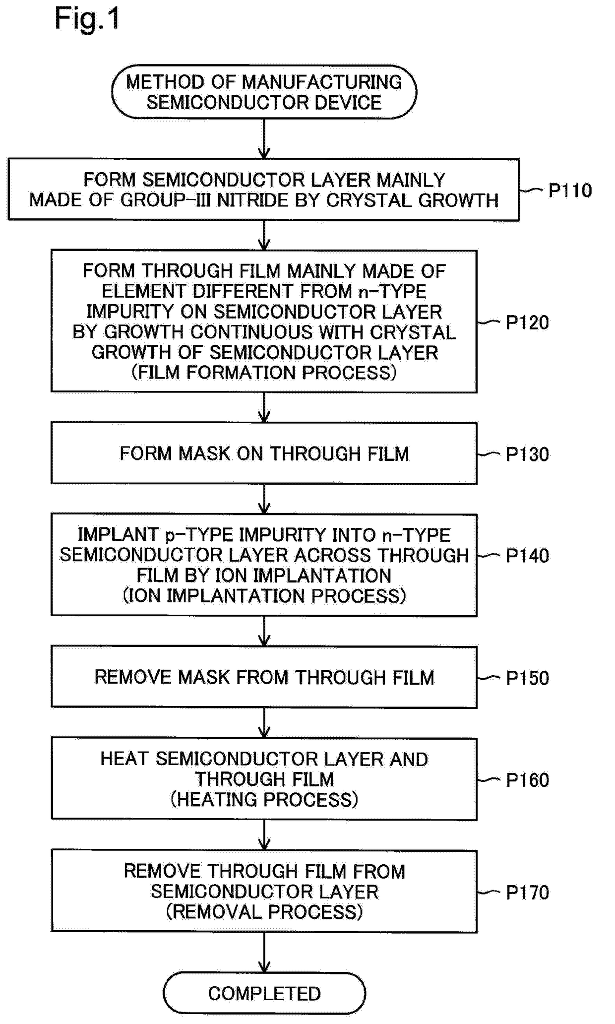
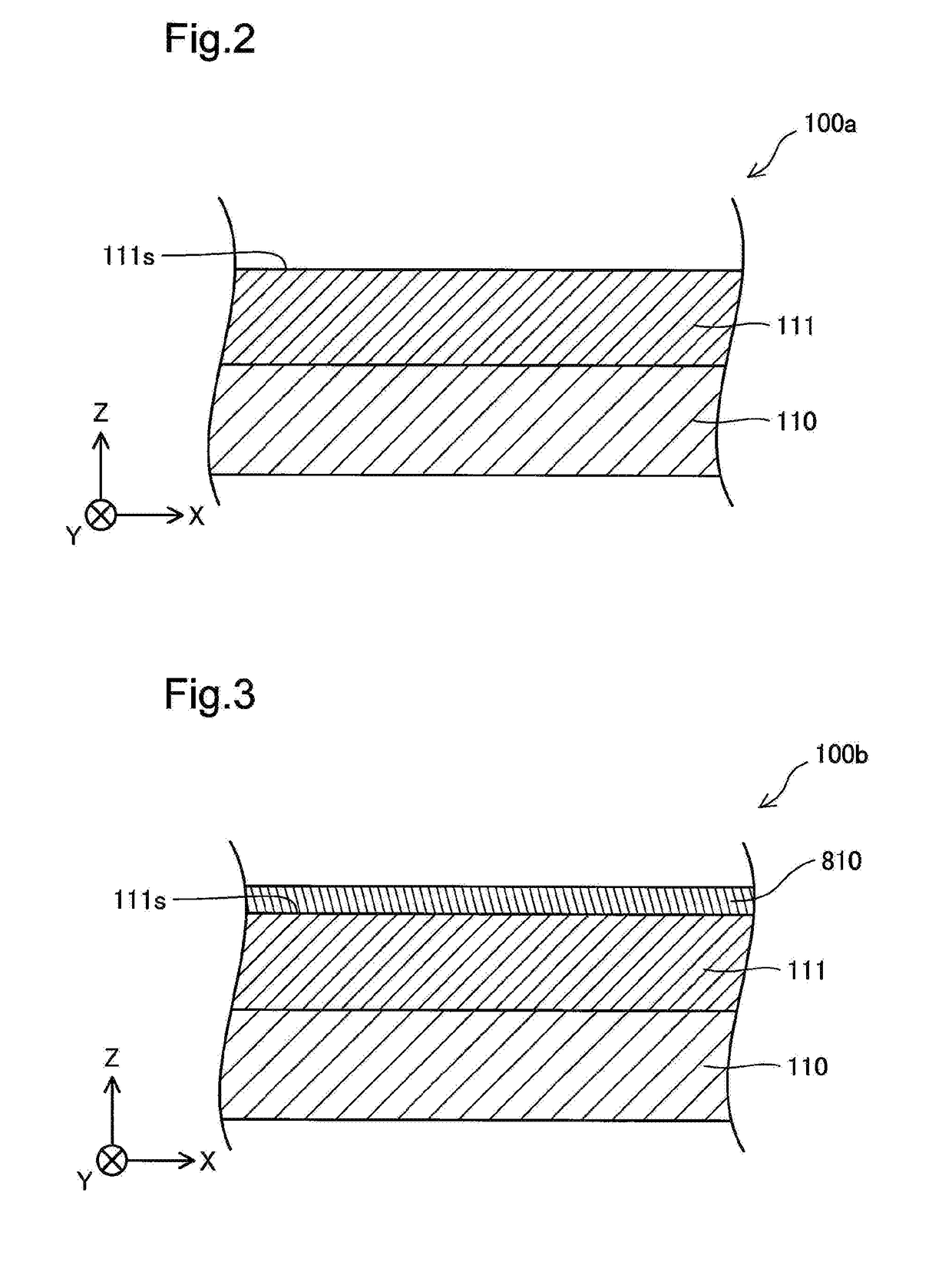
[0046]FIG. 1 is a process chart showing a method of manufacturing a semiconductor device. FIGS. 2 to 8 are diagrams schematically illustrating processes of manufacturing the semiconductor device.

[0047]XYZ axes orthogonal to one another are illustrated in FIG. 2. Among the XYZ axes of FIG. 2, the X axis denotes a left-right axis on the sheet surface of FIG. 2. +X-axis direction denotes a rightward direction on the sheet surface, and −X-axis direction denotes a leftward direction on the sheet surface. Among the XYZ axes of FIG. 2, the Y axis denotes a front-back axis on the sheet surface of FIG. 2. +Y-axis direction denotes a backward direction on the sheet surface, and −Y-axis direction denotes a forward direction on the sheet surface. Among the XYZ axes of FIG. 2, the Z axis denotes a top-bottom axis on the sheet surface of FIG. 2. +Z-axis direction denotes an upward direction on the sheet surface, and −Z-axis direc...

second embodiment

B. Second Embodiment

[0093]FIG. 14 is a sectional view schematically illustrating the configuration of a semiconductor device 200 according to a second embodiment. XYZ axes orthogonal to one another are illustrated in FIG. 14, similarly to FIG. 2.

[0094]According to this embodiment, the semiconductor device 200 is a GaN-based semiconductor device formed using gallium nitride (GaN). According to this embodiment, the semiconductor device 200 is a vertical trench MOSFET (metal-oxide-semiconductor field-effect transistor). According to this embodiment, the semiconductor device 200 is used for power control and is also called power device.

[0095]The semiconductor device 200 includes a substrate 210, a semiconductor layer 211, a p-type semiconductor layer 214 and an n-type semiconductor layer 216. The semiconductor layer 211 includes an n-type semiconductor region 211n and a p-type semiconductor region 211p. The semiconductor device 200 has a trench 222 and recesses 224 as the structures for...

third embodiment

C. Third Embodiment

[0113]FIG. 16 is a sectional view schematically illustrating the configuration of a semiconductor device 300 according to a third embodiment. XYZ axes orthogonal to one another are illustrated in FIG. 16, similarly to FIG. 2.

[0114]According to this embodiment, the semiconductor device 300 is a GaN-based semiconductor device formed using gallium nitride (GaN). According to this embodiment, the semiconductor device 300 is a vertical Schottky barrier diode. According to this embodiment, the semiconductor device 300 is used for power control and is also called power device.

[0115]The semiconductor device 300 includes a substrate 310, a semiconductor layer 311, a Schottky electrode 343, an insulating film 330 and a rear-face electrode 345. The semiconductor device 300 has a mesa 311m as a structure formed in the semiconductor layer 311.

[0116]The substrate 310 of the semiconductor device 300 is similar to the substrate 110 of the first embodiment. The semiconductor layer...


PUM

PropertyMeasurementUnit
temperatureaaaaaaaaaa
pressureaaaaaaaaaa

Abstract

There is provided a method of manufacturing a semiconductor device. The method of manufacturing the semiconductor device comprises a process of forming a semiconductor layer that is mainly made of a group III nitride and has n-type characteristics, by crystal growth; a film formation process of forming a through film that is mainly made of an element different from an element serving as an n-type impurity relative to the group III nitride, by growth on the semiconductor layer continuous with crystal growth of the semiconductor layer; an ion implantation process of implanting a p-type impurity into the semiconductor layer across the through film by ion implantation; a heating process of heating the semiconductor layer and the through film after completion of the ion implantation process, so as to activate a region of the semiconductor layer in which the p-type impurity is ion-implanted, to a p-type semiconductor region; and a removal process of removing the through film from the semiconductor layer, after completion of the heating process. This configuration improves the surface morphology of the p-type semiconductor region formed by ion implantation.

Description

CROSS-REFERENCE TO RELATED APPLICATION[0001]The present application claims priority from Japanese patent application No. 2015-178200 filed on Sep. 10, 2015, the entirety of disclosures of which is hereby incorporated by reference into this application.BACKGROUND[0002]Technical Field[0003]The present invention relates to a semiconductor device, a method of manufacturing the same and a power converter.[0004]Related Art[0005]A known configuration of a semiconductor device (semiconductor element) includes a semiconductor layer formed from a group III nitride such as gallium nitride (GaN). JP 2014-41917A describes a technique that forms a group III nitride-based p-type semiconductor by ion implantation. The technique described in JP 2014-41917A directly implants a p-type impurity into a semiconductor layer by ion implantation, so as to form a p-type semiconductor in a region of the semiconductor layer in which the p-type impurity is ion-implanted.[0006]In the technique disclosed in JP 20...

Claims


Application Information

Patent Timeline
Patent Type & Authority Applications(United States)
IPC IPC(8): H02M7/00H01L29/20H01L21/265H01L21/324H02M7/04H01L21/02
CPCH02M7/003H02M7/04H01L29/2003H01L21/2654H01L21/3245H01L21/0254H02M1/4233H01L29/66212H01L29/872H01L29/0619H01L29/0661H01L21/26553Y02B70/10H01L29/0657
Inventor FUJII, TAKAHIRONIWA, TAKAKI
Owner TOYODA GOSEI CO LTD
Why Eureka
Try Eureka